

PCB Layer Stackup – A Practical Guide (Part 1 – Technical Fundamentals)
PCB Layer Stackup – A Practical Guide (Part 1 – Technical Fundamentals)
Lorenzo Martini, 16/09/2025
In the era of miniaturized electronics and ever-increasing operating frequencies, the arrangement of layers in printed circuit boards (PCBs) is a fundamental design decision that directly affects performance, reliability and cost. While the earliest printed circuit boards were simple single-layer structures, technological evolution has led to the widespread use of increasingly complex multi-layer PCBs, capable of supporting component densities and operating frequencies that would have been unthinkable just a few decades ago.
Stackup design (the arrangement of the layers) has become a sophisticated discipline that balances electrical, thermal, mechanical and economic considerations. An optimal configuration can significantly improve signal integrity, reduce electromagnetic emissions and simplify the manufacturing process, while poor choices can cause malfunctions, EMC failures and excessive production costs.
The shift from single-layer to multi-layer structures isn’t just an incremental technical evolution — it’s a true paradigm shift in electronic design. With each additional layer, complexity grows exponentially, creating new opportunities but also new challenges. In this context, a deep understanding of how the different layers interact becomes essential for every designer.
So what are the fundamental principles that guide effective stackup design? How can configurations be optimized for specific applications? This article explores the fundamental strategies for correct layer arrangement in modern PCBs, offering practical guidelines for designers at different levels and for technical decision-makers who need to understand the implications of these architectural choices.
Stackup Fundamentals
A multi-layer PCB is essentially made up of conductive layers (typically copper) alternating with insulating materials (substrates). The arrangement of these layers, known as the “stackup”, determines many of the final circuit’s electrical, thermal and mechanical characteristics.
The insulating materials, often called “prepreg” and “core”, differ mainly in their processing state: the core is already fully cured, while the prepreg solidifies during the lamination process. This distinction has significant consequences for the final PCB’s dimensional stability and electrical characteristics.
Layers in a PCB can be classified into four main types:
- Signal layers: dedicated to transmitting signals between components
- Power planes: provide power distribution (12V, 3.3V, etc.)
- Ground planes: provide a common reference and return paths for signals
- Mixed layers: combine signals and portions of a plane (typical in PCBs with fewer layers)
Layer symmetry is a fundamental principle for preventing PCB warpage during thermal manufacturing processes. A symmetric stackup distributes thermal stress evenly, significantly reducing the risk of warping and twisting. This symmetry applies not only to the number of layers but also to the copper distribution, which should be balanced with respect to the PCB’s center plane.
The continuity of reference planes is a decisive factor for stackup effectiveness. A fragmented plane can compromise signal integrity, creating unpredictable current return paths. In high-frequency PCBs, return paths tend to follow the “path of least inductance” principle, sitting directly under the outbound trace. A break in the reference plane forces the current into detours that enlarge the loop area, increasing emissions and susceptibility to interference.
One often-overlooked aspect is the “critical spacing” between layers, which affects several electrical parameters. Optimizing this distance, particularly between signal layers and their reference planes, contributes significantly to overall PCB performance, especially in terms of noise immunity and signal integrity.
Common Configurations for Different Layer Counts
2-Layer PCBs
The simplest configuration after single-layer includes:
Layer 1 (Top): typically components and signals
Layer 2 (Bottom): mostly signals and occasionally components
A single substrate between the two layers
This configuration is cheap and suitable for simple low-frequency circuits, but has significant limitations for signal integrity and EMI management.
The absence of a dedicated reference plane in 2-layer PCBs forces special considerations during routing. An effective practice is to create ground areas as wide as possible, especially under critical components such as oscillators or voltage regulators. In low-speed digital circuits, it’s common to use a grid of ground traces that forms a sort of “pseudo-plane”, improving EMI performance without requiring additional layers.
In 2-layer PCBs, routing strategy takes on major importance. An effective approach is to place critical signals on the top layer, keeping the bottom layer for less sensitive signals and for a ground distribution that stays as continuous as possible. Orthogonal trace orientation between the two layers (horizontal on top, vertical on bottom or vice versa) reduces interference between crossing signals.
Application case: smart home thermostat

A smart thermostat is a perfect example of a 2-layer application. The circuit typically includes a low-power microcontroller, environmental sensors and a user interface, all operating at relatively low frequencies (below 20 MHz).
In this device, the top layer hosts the microcontroller and the main components, with a dedicated ground area under the oscillator. Analog signals from the temperature sensors are routed on the top layer with short, direct paths, while the bottom layer mostly holds a ground distribution and the connections to the user interface.
To improve signal integrity, the designer implemented the following strategies:
- Separation of analog and digital circuits with distinct ground zones
- “T” routing to minimize stubs on critical connections
- Strategically placed decoupling components
- Partial ground plane under the analog sensors to reduce noise
This approach delivered reliable performance while keeping production costs contained — a key aspect for a consumer product.
Multi-layer PCBs
Minimizing the space between a signal’s path and its return current to the source is an essential goal for reducing EMI, and becomes mandatory as signal frequencies rise: it’s obvious that respecting this rule is practically impossible in a 2-layer circuit. One remedy is to add ground planes very close to the signal layers, allowing currents to find their optimal return path and minimizing the loop area formed by the outbound and return paths of the current associated with a given signal. Adding planes also enables optimal power distribution, giving currents minimum-impedance paths and creating — together with the ground planes — a distributed capacitance that acts as a low-pass filter.
4-Layer PCBs
A very common configuration for medium-complexity applications is:
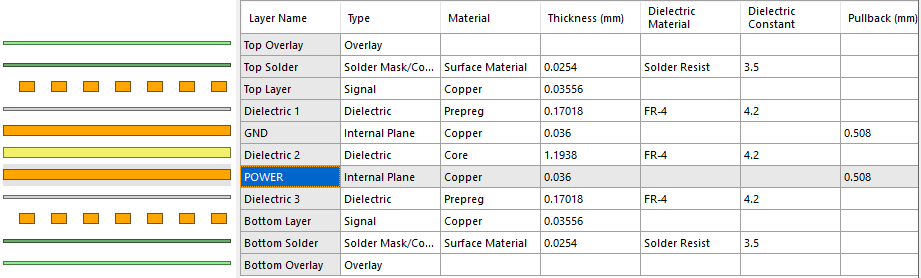 Layer 1 (Top): Signal
Layer 2 (Inner Plane): GND
Layer 3 (Inner Plane): Power
Layer 4 (Bottom): Signal
This stackup offers:
- Uniform power distribution
- A good ground reference for the signals
- Capacitive coupling between power and ground planes
- Well-defined current return paths
Placing planes inside the stackup offers a further benefit: intrinsic shielding. The inner planes, especially the ground plane, act as electromagnetic barriers, reducing coupling between the outer signal layers and improving overall EMC.
A crucial aspect of 4-layer PCBs is the management of layer transitions (vias). Every via represents an impedance discontinuity that can compromise signal integrity at high frequencies. Careful via placement, especially for critical signals, contributes significantly to the circuit’s overall performance.
In the stackup described above, the proximity of the top signal layer to a ground plane optimizes current return paths and creates a controlled transmission system, drastically reducing emissions and crosstalk. That optimization, however, isn’t replicated on the bottom signal layer. For applications more sensitive to interference, an optimized variant could be:
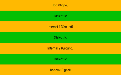
Layer 1 (Top): Signal
Layer 2 (Inner Plane): GND
Layer 3 (Inner Plane): GND
Layer 4 (Bottom): Signal
with power planes implemented partially on layers 1 and 4. This configuration, known as “power islands”, further improves signal integrity at the expense of a less efficient power distribution.
Other configurations are of course possible, including the swap between the bottom layer and the adjacent inner ground plane (layer 3), in order to “bury” the signal traces and shield them further (striplines), raising the frequencies the board can handle.
Application case: industrial data acquisition system
An industrial data acquisition system is an ideal application for a 4-layer PCB. The device includes precision analog-to-digital converters, a digital signal processor (DSP) and communication interfaces operating at intermediate frequencies (50-100 MHz).
In this project, the stackup was optimized as follows:
Layer 1 (Top): Components and analog signals, with dedicated areas for fast digital signals
Layer 2 (GND): Continuous ground plane with no breaks
Layer 3 (Power): Multiple segmented power planes (3.3V digital, 5V analog, etc.)
Layer 4 (Bottom): Mostly digital signals and less critical interconnects
To ensure signal integrity, the designer implemented advanced strategies:
- Differential routing for fast serial interfaces
- Physical separation between analog and digital sections
- Via stitching to effectively connect the ground planes between layers 1 and 2
- Segmented power plane on layer 3 to isolate different power domains
This configuration delivered excellent rejection of ambient noise — essential in industrial environments — while keeping production costs reasonable for a mid-range device.
6-Layer PCBs
The ever-increasing price pressure, especially from Asian PCB manufacturers, has made 6-layer stackups a good compromise between cost and performance for more complex applications. The miniaturization of circuits and the dizzying increase in chip pin counts needed to access signals demands a further increase in PCB layers to properly route the connection traces. One possible configuration that prioritizes the number of signal layers is:
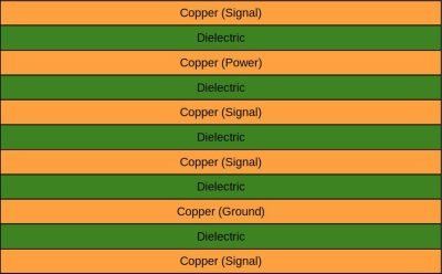 Layer 1 (Top): Signal
Layer 2 (Inner Plane): Power
Layer 3 (Inner Plane): Signal
Layer 4 (Inner Plane): Signal
Layer 5 (Inner Plane): GND
Layer 6 (Bottom): Signal
However, such a configuration doesn’t sit well — given what we’ve seen about optimizing current return paths — with handling high-frequency signals or avoiding potential cross-talk and general EMI issues. For better EMC performance while still aiming for an optimized power distribution, you can adopt this configuration:
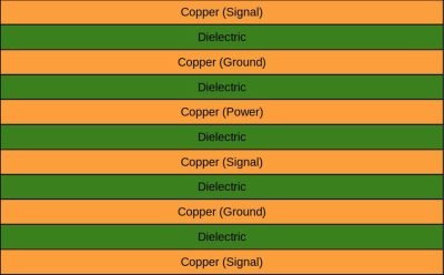 Layer 1 (Top): Signal
Layer 2 (Inner Plane): GND
Layer 3 (Inner Plane): Power
Layer 4 (Inner Plane): Signal
Layer 5 (Inner Plane): GND
Layer 6 (Bottom): Signal
Adding two layers compared to the 4-layer configuration introduces significant flexibility in signal management. Internal layers can be dedicated to specific signals, such as data buses or high-speed clocks, benefiting from the shielding offered by adjacent planes.
In a 6-layer stackup, impedance management becomes more sophisticated. The inner layers allow the use of striplines (transmission lines fully enclosed between reference planes), which offer better immunity to interference than microstrips on the outer layers. This supports a more robust design for high-speed signals.
The choice between the two configurations presented depends mainly on the specific project requirements. As noted, the first configuration maximizes the surface area available for routing, while the second optimizes shielding and power distribution. The latter is preferable for applications with strict EMC requirements or high operating frequencies.
An important aspect of 6-layer design is thermal management. As component density and power dissipation rise, ground and power planes can play a crucial role in distributing heat. A careful thermal design that includes strategically placed thermal vias contributes to device longevity and reliability.
Application case: industrial IoT gateway
 An industrial IoT gateway is an emblematic application for a 6-layer PCB. The device integrates a performant processor, high-speed memory, multiple communication interfaces (Ethernet, Wi-Fi, cellular) and complex power-supply circuitry.
In this project, the stackup was configured as follows:
- Layer 1 (Top): Main components and high-frequency signals (Wi-Fi, RF)
- Layer 2 (GND): Continuous ground plane
- Layer 3 (Signal): Memory buses and fast digital signals
- Layer 4 (Power): Distribution of multiple voltages with segmentation
- Layer 5 (GND): Second ground plane
- Layer 6 (Bottom): Secondary components and less critical signals
The design incorporated advanced techniques:
- Impedance control for all differential signals (USB, Ethernet)
- “Picket fence” routing to minimize crosstalk between parallel signals
- RF isolation with “fence via” structures around the wireless circuits
- Dedicated power zones with localized filtering
Adopting a 6-layer PCB made it possible to effectively manage the high complexity of the system, while ensuring excellent EMC performance and reliability in demanding industrial environments.
8+ Layer PCBs
For high-complexity, high-frequency applications, stackups with 8, 10, 12 or more layers offer:
- Separation of critical signals
- Multiple power supplies
- Improved shielding
- Greater routing flexibility
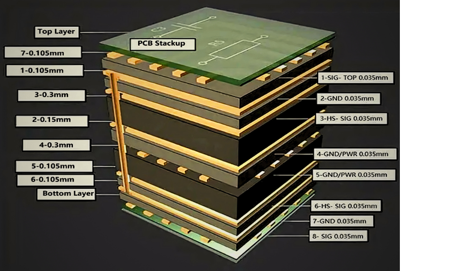
** An example of an 8-layer stackup might be:**
- Layer 1 (Top): Signal
- Layer 2 (Inner layer): GND
- Layer 3 (Inner layer): Signal
- Layer 4 (Inner layer): Power
- Layer 5 (Inner layer): GND
- Layer 6 (Inner layer): Signal
- Layer 7 (Inner layer): GND
- Layer 8 (Bottom): Signal
As the layer count grows, design complexity rises significantly — but so do the possibilities. Multiple ground and power planes enable sophisticated segmentation of power domains, essential for systems that integrate analog, digital and RF circuits in close proximity.
In advanced stackups, the concept of “vertical segregation” becomes fundamental. Signals can be organized not only by functional domain (analog, digital, power) but also by criticality level or frequency band. For example, high-speed signals can be confined to specific layers optimized for those applications.
Redundancy of reference planes dramatically improves the electromagnetic robustness of the system. In applications with strict immunity or low-emission requirements, this characteristic can be decisive for project success, eliminating the need for costly external shielding or additional filters — all of which must be factored into the product budget.
A distinguishing feature of advanced stackups is the ability to implement specialized guided structures, such as asymmetric striplines or broadside-coupled lines, which offer superior electrical characteristics for critical applications. These configurations require careful design and collaboration with the PCB manufacturer, but they can offer significant performance advantages.
Application case: satellite communication system
A satellite communication terminal is a paradigmatic example of an application that requires a 10-layer PCB. The system integrates high-frequency RF sections (up to 12 GHz), complex digital signal processing and sophisticated power management.
 In this advanced project, the stackup was designed as follows:
- Layer 1 (Top): RF components and microwave circuits
- Layer 2 (GND): Dedicated RF ground plane
- Layer 3 (Signal): Controlled RF transmission lines
- Layer 4 (GND): Isolation ground plane
- Layer 5 (Power): Analog power distribution
- Layer 6 (GND): Central ground plane
- Layer 7 (Signal): High-speed data buses
- Layer 8 (Power): Digital power distribution
- Layer 9 (GND): Digital ground plane
- Layer 10 (Bottom): Digital circuits and support components
This configuration implements a complete segregation between RF, analog and digital circuits, with dedicated ground planes for each domain. Advanced strategies include:
- Optimized transitions between microstrip and stripline for microwave signals
- Resonant structures embedded in the inner layers for RF filtering
- Thermal distribution via a planned network of thermal vias
- Compartmental shielding between sensitive sections
Adopting such a sophisticated PCB made it possible to integrate into a single device functions that would traditionally have required multiple separate boards, reducing size, weight and power consumption — all critical aspects for space applications.
Advanced Principles of Layer Arrangement
Plane Coupling
The distance between power and ground planes has a significant impact on the distributed bypass capacitance, which naturally filters noise. A thinner dielectric between these planes increases the decoupling capacitance and improves high-frequency performance.
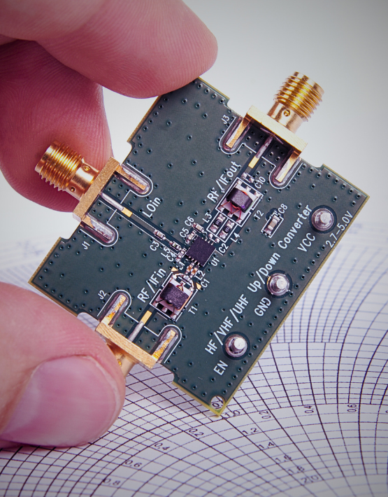 The capacitive effect between adjacent planes isn’t a secondary phenomenon — it’s a fundamental design feature that can be strategically exploited. The distributed capacitance between power and ground planes creates a natural filtering system that can be quantified and optimized. For a typical digital system, this capacitance is around 75-100 pF per square inch — a value that can be significantly increased by reducing the dielectric thickness or using materials with a high dielectric constant.
Beyond distance, the continuity of the planes and their structural integrity directly influence how effective this coupling is. Slots in the planes, needed for vias or isolation, create discontinuities that can compromise high-frequency performance. Techniques like “via stitching” and “moats” let you maintain plane integrity while respecting electrical isolation constraints.
In high-speed systems, plane coupling contributes to the stability of the power distribution impedance. A low impedance in the power distribution network (PDN) is essential to minimize simultaneous switching noise (SSN), a phenomenon that becomes critical as switching speeds and the number of switching buffers increase.
Practical application: noise reduction in a high-performance FPGA
In a system based on an FPGA running at 500 MHz, optimizing plane coupling made it possible to significantly reduce power-supply noise. The designer implemented:
- Reduced dielectric thickness between power and ground planes to 100 μm
- Use of a material with εr = 4.5 to increase the distributed capacitance
- Strategic segmentation of the power planes with minimal interruptions
- Bypass capacitor network designed considering the intrinsic distributed capacitance
This strategy made it possible to keep the PDN impedance below 50 mΩ in the critical band (10 MHz – 1 GHz), significantly improving signal integrity and reducing EMI emissions by 12 dB compared to the previous design.
Controlled Impedance
For high-speed signals, it’s essential to keep a constant characteristic impedance along the entire path. Impedance control depends on:
- Trace width
- Copper thickness
- Distance from the reference plane
- Dielectric constant of the substrate
CHARACTERISTIC IMPEDANCE CALCULATION FOR A TRACE
For a microstrip:
Z₀ = (87 / √(εᵣ + 1.41)) × ln(5.98 × h / (0.8 × w + t))
Where:
- Z₀ = characteristic impedance in Ohms
- εᵣ = relative dielectric constant of the substrate
- h = height from the reference plane
- w = trace width
- t = copper thickness
For a stripline, the formula becomes more complex:
Z₀ = (60 / √εᵣ) × ln(4h / (0.67 × π × (0.8w + t)))
Where:
- h = distance between the reference planes
- w = trace width
- t = copper thickness
These formulas provide useful approximations for preliminary estimates, but for precise calculations it’s recommended to use electromagnetic simulators or the calculation tools provided by PCB manufacturers, which also account for secondary effects such as copper roughness and the dispersive properties of the material.
Characteristic impedance is a fundamental property of transmission lines on PCBs, and managing it goes well beyond simply specifying a trace width. Uncontrolled or poorly designed impedance causes reflections that degrade signal integrity, producing effects such as ringing, overshoot and timing jitter.
In practical design, impedance control requires close collaboration with the PCB manufacturer. Manufacturing tolerances, in particular those relating to copper and dielectric thickness, directly affect the resulting impedance. A robust design should account for these variations, implementing an adequate safety margin.
The most common transmission structures in multi-layer PCBs are:
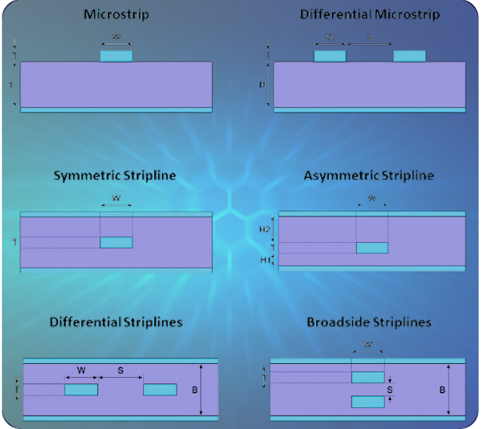
- Microstrip: traces on the outer layer with a single reference plane
- Stripline: traces on an inner layer between two reference planes
- Dual stripline: two signal layers sharing the same reference planes
- Asymmetric stripline: similar to stripline but with different distances from the reference planes
Each configuration has specific advantages in terms of performance, routing density and ease of manufacturing. The choice of the optimal structure depends on the specific signal requirements and overall project constraints.
Application: high-speed DDR4 interface
In an advanced processing system with DDR4-3200 memory, impedance control proved crucial for ensuring signal integrity at 1600 MHz. The designer implemented:
- 100 Ω differential traces (±5%) for DQS signals
- 50 Ω single-ended traces (±5%) for DQ and command signals
- Microstrip on outer layers to ease termination
- Stripline on inner layers for critical signals with tighter crosstalk tolerance
The process included:
- Preliminary simulation with different stackups and geometries
- Collaboration with the manufacturer to define achievable parameters
- Fabrication of test coupons on the production panel
- Impedance verification via TDR (Time Domain Reflectometry)
This attention to impedance control allowed a timing margin more than 10% above the minimum requirements, ensuring reliable operation even under varying environmental conditions.
Distribution of Critical Signals
High-speed or sensitive signals should be:

- Placed close to continuous reference planes
- Separated from potentially interfering signals
- Routed on inner layers whenever possible
- Grouped by type and frequency
Optimal distribution of signals within the stackup is one of the most complex challenges in advanced PCB design. Every placement decision affects not just the performance of a single signal but the entire electromagnetic ecosystem of the circuit.
A fundamental principle is segregation by functional and frequency domains. Low-frequency analog signals, fast digital signals and power circuits should occupy distinct areas of the PCB, with well-defined boundaries. This separation also extends vertically through the stackup, with layers dedicated to specific categories of signals.
For high-speed signals, the distribution must also consider the current return paths. According to transmission-line theory, the return current follows the minimum-impedance path, which at high frequencies coincides with the area directly under the trace. Breaks in this path (slots in planes, changes of reference plane) generate extended current loops that increase emissions and susceptibility.
The distribution should also minimize critical paths. Clock, reset and synchronous control signals deserve particular attention, with routing optimized to minimize length and skew. Techniques such as “length matching” and “delay tuning” become essential to ensure correct timing in high-speed systems.
Practical application: medical imaging acquisition system
In a precision medical imaging system, signal distribution was optimized to ensure signal integrity and minimize interference:
- Analog sensor signals routed exclusively on layer 3, shielded by two ground planes
- High-frequency clock lines (125 MHz) isolated on layer 6 with guard traces on both sides
- High-speed data buses distributed on layers 4 and 5 as differential striplines
- Switching power circuits confined to a dedicated PCB area with local shielding
For the most critical signals, the designer implemented:
- Analog voltage references routed as a “star topology” to minimize interference
- Critical nets individually identified and simulated with signal-integrity analysis
- Via shielding through “picket fence” structures for layer transitions
- “H-tree” topology for the main clock distribution
These strategies achieved a signal-to-noise ratio above 90 dB in the analog circuits — essential for the system’s diagnostic accuracy — while keeping EMI emissions well below regulatory limits for medical devices.
Conclusion
Stackup design is a fundamental architectural decision that influences the entire life cycle of an electronic product. An optimal layer arrangement balances electrical, thermal, mechanical and economic requirements, offering a competitive advantage in terms of performance, reliability and time-to-market.
The stackup isn’t just a technical aspect of design, but a strategic decision that defines the fundamental capabilities and limits of an electronic system. The increasing complexity of modern devices, integrating different technologies (digital, analog, RF, power) into ever smaller spaces, makes this architectural decision even more critical.
The optimal approach to stackup design requires a holistic view that integrates different perspectives: the electrical needs of signal integrity and electromagnetic compatibility, the thermal requirements for efficient heat dissipation, the mechanical constraints for strength and stability, and the economic considerations related to cost and manufacturability.
For designers, it’s essential to consider the stackup in the earliest stages of the development process, collaborating closely with PCB manufacturers to ensure feasibility and cost optimization. For decision-makers, understanding the impact of the stackup on the final product’s performance allows for appropriate resource allocation and realistic specifications.
The fundamental principles presented in this article — symmetry, appropriate segmentation, impedance control, and optimal signal distribution — provide a solid basis for tackling this design challenge. However, every application presents unique characteristics that require specific considerations and, often, carefully weighed trade-offs.
In a continuously evolving technological context, the ability to design optimized stackups becomes a strategic skill that differentiates excellent products from mediocre ones. Companies that invest in this competence can achieve significant advantages in terms of quality, cost and development speed.
Emerging trends in materials and interconnect technologies promise to further expand the possibilities, enabling ever higher performance in ever smaller spaces. Designers who thoroughly understand the fundamental principles of stackup design will be better equipped to leverage these innovations and develop the next generation of electronic products.
In Part 2 of this guide we’ll dive into the economic considerations that should be weighed before deciding which stackup to adopt, so you take into account not only the PCB cost but the so-called TCO (Total Cost of Ownership) of the product. We’ll walk through another round of application examples and the evolutionary trends in stackups driven by advancing technology.
Stay tuned!