

Mastering Noise in Analog Circuits: Advanced Strategies for Superior Performance
Mastering Noise in Analog Circuits: Advanced Strategies for Superior Performance
- Lorenzo Martini – 01/08/2025
The Phenomenon of Noise: A Constant Challenge in Analog Design
Electronic noise is one of the most insidious problems that electronics engineers deal with every day. This seemingly invisible phenomenon can irreparably compromise the performance of an analog circuit, causing inconsistencies in data transmission, measurement errors, and signal quality degradation. But what are the real implications of noise in a professional setting?
In industrial environments, a control system affected by noise can cause erroneous sensor readings, with consequent automated decisions that can be harmful to the entire production process. In the medical sector, where precision is fundamental, noise can mask critical biological signals, leading to imprecise diagnoses. It’s clear, then, that understanding and controlling electronic noise isn’t just an option — it’s an absolute necessity for any circuit designer.
Fundamentals of Electronic Noise: A Mix of Components
Electronic noise isn’t a single entity but a complex set of phenomena with different origins and behaviors. By analyzing the main types in depth, we can develop targeted strategies to counter them effectively.
Thermal Noise: The Unavoidable Component
Thermal noise, also known as Johnson-Nyquist noise, comes from the random motion of electrons in conductive materials at temperatures above absolute zero. Its RMS voltage can be calculated precisely with the formula:
Vnrms = √(4kTRΔf)
Where:
-
k is the Boltzmann constant (1.38 × 10⁻²³ J/K)
-
T is the absolute temperature in Kelvin
-
R is the resistance in ohms
-
Δf is the bandwidth in Hertz
In a concrete application, consider a precision amplifier operating at room temperature (25 °C / 298K) with a 10kΩ input resistance and a 100kHz bandwidth. The thermal noise generated will be about 4μV RMS — a value that may seem negligible but becomes significant when working with signals on the order of microvolts, as in biomedical sensors.
Shot Noise: The Quantum Signature of Current
Shot noise derives from the discrete nature of electric charge. When charge carriers cross a junction, as in a diode or a bipolar transistor, they generate statistical fluctuations in the current. The amplitude of this noise is proportional to the square root of the average current:
Inrms = √(2qIΔf)
Where:
-
q is the electron charge (1.602 × 10⁻¹⁹ C)
-
I is the average current
-
Δf is the bandwidth
A practical example shows up in the photodiodes used to receive optical signals. In a fiber-optic communication system operating with a photodiode generating 1mA of current, the associated shot noise in a 1MHz band will be about 18nA RMS — a limiting factor for the link’s signal-to-noise ratio.
Flicker Noise (also known as 1/f): The Low-Frequency Dominator
Flicker noise is a particular challenge because its spectral density increases as frequency decreases, following a 1/f relationship. Its origins are multiple and often tied to structural imperfections in semiconductor materials.
Consider an analog-to-digital converter in an environmental data acquisition system that samples at low frequency (1Hz). Flicker noise in this context will be significantly higher than thermal noise, potentially masking subtle but important variations in the monitored parameters. For this reason, in such applications it’s essential to implement techniques like chopping or autozero to mitigate the effect of flicker noise.
Burst (Popcorn) Noise: The Unpredictable Element
Burst noise, sometimes called “popcorn” for its impulsive behavior, shows up as sudden jumps in the signal level. It’s primarily caused by defects in the crystalline structure of semiconductors and by the capture/release of charge carriers in impurity zones.
An emblematic case is that of preamplifiers for precision microphones, where burst noise can introduce audible “clicks” in a recording. In a professional sound-recording installation, this phenomenon can render an entire session unusable, with significant financial losses.
But how do you quantify noise in circuits?
Quantifying noise in electronic circuits is fundamental for evaluating system performance and determining the most effective mitigation strategies. Several metrics and units are used, each appropriate for a specific context.
Noise Spectral Density
Noise spectral density represents the distribution of noise as a function of frequency and is one of the most widely used metrics:
-
For voltage noise: nV/√Hz (nanovolts per square root hertz)
-
For current noise: pA/√Hz (picoamperes per square root hertz)
This measurement is particularly useful because it’s independent of bandwidth, allowing direct comparisons between different devices. For example, a high-quality op-amp might have a voltage noise spectral density of 1 nV/√Hz at 1 kHz.
RMS Noise Voltage or Current
For measurements within a specific frequency band, we use the RMS (Root Mean Square) value:
-
Noise voltage: μV RMS or nV RMS
-
Noise current: μA RMS or nA RMS
The RMS value is related to spectral density by: Vnoise(RMS) = Vn × √(bandwidth)
Noise Equivalent Power (NEP)
Used primarily for optical detectors and sensors, measured in W/√Hz (watts per square root hertz).
Noise Figure
The noise figure is a dimensionless parameter that quantifies the degradation of the signal-to-noise ratio caused by a component or system, expressed in dB:
NF = 10 × log₁₀(SNR_input / SNR_output)
An ideal amplifier would have a noise figure of 0 dB. Typical values for real amplifiers range from 1-2 dB (excellent) to 10+ dB (mediocre).
SNR (Signal-to-Noise Ratio)
Defines the signal-to-noise ratio. It’s measured in dB and calculated as follows:
SNR = 10 × log₁₀(Signal Power / Noise Power)
Where powers are typically measured in watts or volts² for systems with constant impedance. The higher the value, the “cleaner” the signal — that is, the less masked by noise.
*SINAD (Signal-to-Noise-and-Distortion Ratio)*
Signal-to-noise-and-distortion ratio, including both random noise and harmonic distortion. It’s measured in dB, sometimes expressed as dBsinad, and calculated as:
SINAD = 10 × log₁₀(Signal Power / (Noise Power + Distortion Power))
Where powers are typically measured in watts or volts² for systems with constant impedance. Note that, by including distortion, SINAD is always ≤ SNR (Signal-to-Noise Ratio), which considers only the noise. SINAD is preferred for evaluating the overall signal quality in systems where distortion is not negligible, such as ADCs, DACs, or non-linear amplifiers.
Practical Strategies for Noise Control: From Analysis to Implementation
Effective noise management requires a systematic approach that begins in the design phase and continues through implementation and testing of the circuit.
Critical Component Selection: The First Step Toward Quality
Choosing the right components is the foundation of any effective anti-noise strategy. But what does “low-noise component” really mean in specific application contexts? In the case of resistors, metal-film types offer significantly better noise performance than carbon resistors. A concrete example: in a preamplifier for ECG signals, swapping carbon resistors for metal-film equivalents in the amplification circuit can reduce the noise floor by up to 6dB, making visible details of the cardiac signal that would otherwise be masked.
For op-amps, in addition to the classic OP27 and AD797, the OPA1612 is worth considering, combining extremely low voltage noise (1.1nV/√Hz at 1kHz) with contained current noise, which makes it ideal for high-precision audio applications and analytical instrumentation.
In the realm of capacitors, it’s not just the ESR (Equivalent Series Resistance) that determines noise performance, but also the stability of the dielectric. Class C0G/NP0 ceramic capacitors offer the best stability and lowest noise, essential in oscillator circuits and precision filters. In a PLL frequency synthesizer, for example, replacing X7R ceramic capacitors with C0G equivalents can improve phase jitter by a factor of 3-5, with immediate benefits for the spectral purity of the generated signal.
PCB Layout: The Scientific Art of Placement
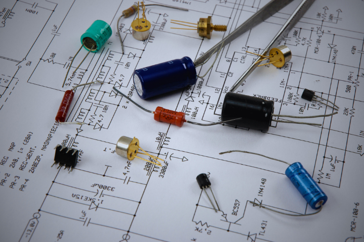 PCB layout carries a critical importance that goes well beyond simply connecting components. What concrete principles should guide a designer in creating a low-noise PCB?
In a recent data acquisition project for precision sensors, adopting a “divide and conquer” approach led to notable results. The circuit was segmented into functional zones (power, analog signals, digital processing) that were physically separated and interconnected through well-defined transition points. This strategy reduced the system noise floor by more than 10dB compared to a previous version built by another supplier using a less structured layout.
Handling critical traces is another fundamental aspect. Traces carrying sensitive analog signals should be as short as possible, kept away from power lines, and surrounded by ground planes that act as shielding. In an amplifier for ultrasonic transducers, rigorous application of these principles let us increase the effective dynamic range by 14dB, significantly improving the resolution of the resulting ultrasound image.
For differential signals, it’s crucial to maintain tight coupling between the traces of the pair, ensuring identical lengths and controlled impedances. This approach minimizes the conversion of common-mode noise into differential noise, preserving signal integrity. A concrete example is LVDS interfaces in image acquisition systems, where careful routing can determine the difference between a clean image and one affected by visible artifacts.
Grounding and Shielding: Effective Defensive Strategies
The concept of ground, apparently simple, hides significant complexity when it comes to managing noise. Which practical approaches have proven most effective?
Star grounding is an elegant solution but one that requires attention in implementation. In a recently developed industrial control system, adopting a star ground with a single reference point eliminated persistent instability problems caused by ground loops. The implementation required physical reorganization of the current returns, with particular attention to the paths of high-frequency digital currents.
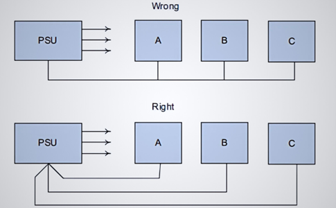
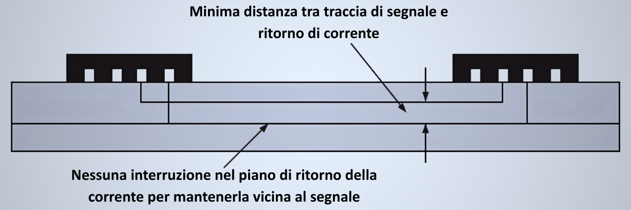
The segmented grounding technique offers a valid alternative in complex systems. It consists of splitting the ground plane into sections dedicated to specific functions (analog, digital, power), interconnected at a single well-defined point. In a professional audio-video system, this approach eliminated audible interference caused by the digital section, without requiring expensive additional shielding. Not everyone agrees on this “traditional” approach, though: managing unified ground planes that are correctly positioned in the circuit’s layer stack-up to minimize the distance between a signal and its return current can yield even better results. The important thing, in that case, is to ensure that the return current path doesn’t separate from the signal path — hence the need for continuous planes.
As for shielding, it’s important to consider both the material and the configuration. For low-frequency electric fields, a conductive shield connected to ground is enough. For magnetic fields, on the other hand, high-permeability materials like mu-metal offer superior performance. In a sensitive installation for magnetometric measurements, adopting a three-layer shield (inner and outer mu-metal with an intermediate copper layer) reduced ambient noise by a factor of 100, making measurements possible that had previously been impossible.
Advanced Filtering Techniques: Practical, Targeted Solutions
Filtering is a versatile tool in the fight against noise. But which topologies offer the best trade-off between effectiveness, complexity, and cost?
Passive filters, RC and LC, offer effective solutions for many applications thanks to their simplicity. In a power supply for precision audio circuits, inserting multiple cascaded RC filters reduced residual ripple from 10mV to less than 100μV, with an audible improvement in sound quality. The key to success was the progressive sizing of the components and the physical separation between filtering stages.
For more demanding applications, active filters offer superior performance, especially when implemented with Butterworth or Chebyshev topologies. In a vibration monitoring system, a 4th-order Butterworth filter implemented with low-noise op-amps allowed seismic signals in the 0.1-10Hz band to be accurately isolated, effectively eliminating high-frequency environmental interference and low-frequency drift.
A particularly effective technique in the presence of noise at a specific frequency is the notch filter. In a laboratory located near a railway line, a notch filter centered at 50Hz eliminated the electromagnetic interference generated by the railway’s power network, enabling precision measurements that had previously been impossible.
_For more on circuit filters, I refer you to the post “Active and Passive Electronic Filters: 6 + 1 application examples_”, specifically dedicated to the subject.*
Advanced Noise Management Techniques: Beyond Conventional Solutions
For systems with particularly stringent requirements, there are techniques that go beyond the conventional approach to the noise problem.
Modulation and Demodulation: The Benefit of Frequency Transposition
The modulation technique offers an elegant solution when working with low-frequency signals affected by flicker noise. Through modulation, the useful signal is shifted to higher frequencies, where 1/f noise is less present.
A concrete example is precision temperature sensors. In a differential scanning calorimetry application, adopting a modulation-demodulation system made it possible to detect temperature variations on the order of 0.001°C — a result impossible with direct measurement techniques due to the flicker noise of the amplifiers. The thermistor signal was modulated at 1kHz by a precision analog switch, amplified, and then synchronously demodulated, achieving an improvement in the signal-to-noise ratio of more than 40dB in long-term measurements.
Differential Amplification and CMRR: The Power of Common-Mode Rejection
Using differential techniques is a fundamental strategy for rejecting noise common to both inputs of an amplifier. The key parameter in this context is CMRR (Common Mode Rejection Ratio), which quantifies the circuit’s ability to discriminate between the differential component (useful signal) and the common-mode component (noise), when the signal is transmitted differentially.
In a recent application, a differential amplifier with CMRR above 100dB made it possible to detect potentials on the order of 50μV in an electrically noisy industrial environment. The implementation required particular attention to matching input impedances and equalizing signal paths.
To maximize CMRR in practical implementations, it’s essential to use precision resistors (0.1% tolerance or better) in the feedback networks and to maintain rigorous balance between signal paths. In especially critical circuits, active trimming techniques can further improve CMRR, reaching values above 120dB.
Advanced-Technology Components: State-of-the-Art Solutions
The evolution of semiconductor technology continuously offers new opportunities for noise reduction. Beyond the traditional JFETs and MOSFETs, HEMTs (High Electron Mobility Transistors) based on materials like GaAs and GaN deserve attention, offering exceptional noise performance at high frequencies.
The literature reports that in a recent radioastronomy application, adopting LNAs (Low Noise Amplifiers) based on HEMT technology reduced the receiver system’s noise temperature from 120K to less than 40K, significantly improving the sensitivity of the radio telescope and enabling observation of cosmic sources previously undetectable.
In the realm of analog-to-digital converters, delta-sigma technology offers significant advantages in terms of quantization noise, especially for band-limited signals. The technologies for moving from the analog world to the digital one and back are quite varied and certainly deserve a deeper look. We’ll publish a post dedicated entirely to the subject soon.
Noise Measurement and Characterization Methods: The Importance of Quantitative Analysis
Effective noise management requires instruments and techniques that allow the phenomenon to be accurately quantified and characterized.
Measurement Instruments and Setup: Practical Approaches
Accurately measuring noise requires attention not only to the instruments used but also to the overall measurement setup. What are the traps to avoid?
The spectrum analyzer is the primary instrument for characterizing noise in the frequency domain. In the analysis of a precision amplifier, using an FFT spectrum analyzer with sample averaging made it possible to identify periodic noise components at 17.5kHz caused by a seemingly well-filtered DC-DC converter. The discovery led to a redesign of the power supply system, with a subsequent improvement in the noise floor of 14dB.
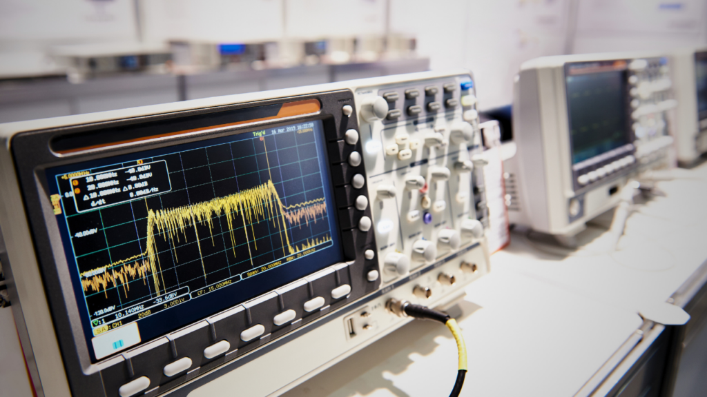
For wideband noise measurements, it’s essential to precisely define the measurement bandwidth and use appropriate filters. A common mistake is making measurements with excessive bandwidth, which leads to overestimating the noise actually present in the band of interest.
Advanced Techniques: Cross-Correlation and Statistical Analysis
For particularly demanding noise measurements, the cross-correlation technique allows you to go beyond the limits imposed by the intrinsic noise of the measurement instruments themselves.
In an electrical metrology laboratory, implementing a cross-correlation-based measurement system made it possible to characterize amplifiers with noise below 0.5nV/√Hz, well below the noise floor of individual measurement instruments. The setup used two identical amplifiers and acquisition systems, combining the results through correlation algorithms that statistically canceled out the uncorrelated noise of the two measurement channels.
Statistical analysis of noise provides valuable information on its nature. While purely thermal or shot noise exhibits a Gaussian distribution, deviations from this statistic can indicate the presence of other noise mechanisms. In analyzing an oscillator circuit, for example, observing a non-Gaussian distribution in the jitter can lead to identifying a coupling problem with other circuits: typically power supply sections or, more generally, switching circuits, where the rapid variations of currents and voltages generate harmonics capable of coupling capacitively or inductively to other signals.
Integrated Case Studies: From Analysis to Solution
To fully understand how the techniques discussed translate into concrete solutions, let’s examine two complete case studies.
Case 1: Data Acquisition System for Precision Sensors

A data acquisition system for precision temperature sensors had an excessive noise floor that limited the effective resolution to about 0.3°C, insufficient for the intended application in a critical thermal control process (target: 0.1 °C resolution). Spectral analysis of the noise revealed three main components:
-
Dominant flicker noise below 10Hz
-
50Hz interference from the electrical grid
-
Broadband noise of thermal origin
The integrated approach to the solution involved:
-
Replacing the op-amps with ultra-low-noise models (LT1028).
-
Implementing a modulation-demodulation system at 400Hz to overcome the flicker noise problem.
-
Adopting battery power for the most sensitive stages, completely eliminating mains interference.
-
Redesigning the PCB with physical separation between analog and digital sections.
-
Implementing active notch filters for the residual 50Hz components.
The final result showed an improvement in effective resolution to 0.07 °C, exceeding the required specifications and allowing significantly more precise process control.
Case 2: Professional Audio Preamplifier
A client told me about a project for a high-quality microphone preamplifier that exhibited excessive background noise, particularly noticeable at high gains, compromising the quality of recordings in quiet environments.
The analysis identified:
-
Significant thermal noise from the bias resistors
-
Inductive coupling between the power transformer and the input stages
-
Shot noise in the input-stage transistors
The solution implemented included:
-
Redesigning the input stage using matched JFETs in a cascode configuration, significantly reducing shot noise.
-
Replacing the critical resistors with low-noise 0.1%-precision metal-film models (reducing thermal noise).
-
Physically relocating the power transformer and introducing mu-metal shielding (reducing electromagnetic noise).
-
Implementing a multi-stage power supply system with progressive filtering (reducing electrical noise).
-
Adding extra ground layers to the circuit’s stack-up (general reduction of electromagnetic noise coupling paths).
The resulting preamplifier showed an improvement in signal-to-noise ratio of more than 10dB, making it highly competitive with the competition in terms of noise performance.
Final Considerations: Toward Low-Noise Design
Effective management of noise in analog circuits isn’t simply a matter of applying predefined formulas and techniques — it requires a systemic approach that integrates theoretical knowledge, practical experience, and rigorous analytical methods. The continuous evolution of electronic technology constantly offers new tools to tackle this challenge, but the fundamental principles remain unchanged:
-
Understanding the noise sources
-
Critical component selection
-
Meticulous attention to layout
-
Implementing techniques appropriate for the specific application
In this context, the ability to accurately measure and characterize noise becomes as fundamental as the ability to design circuits to minimize it. Reaching optimal performance in terms of signal-to-noise ratio almost certainly means factoring in several cycles of analysis, design, implementation, and verification.
For the modern designer, the noise challenge is as much an obstacle as an opportunity: mastering the techniques described in this article not only lets you create better-performing circuits, it opens the door to innovations in fields where the limits imposed by noise have traditionally represented insurmountable barriers.