

PCB Layer Stackup – A Practical Guide (Part 2 – Economic and Application Considerations)
PCB Layer Stackup – A Practical Guide (Part 2 – Economic and Application Considerations)
Lorenzo Martini, 31/10/2025
A Look Back: the Evolution of PCB Stackups
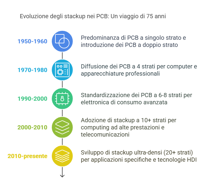 The evolution of PCB stackups is closely tied to the development of electronics over the last 75 years. We can sum up the main evolutionary stages in the diagram below:
This evolution has been driven mainly by component miniaturization, increasing operating frequencies and the need to manage power consumption and thermal dissipation in ever smaller spaces.
Stackup evolution isn’t simply a linear progression toward a higher number of layers — it reflects paradigmatic changes in electronic technology. During the 1960s, the shift from single to double-layer revolutionized the sector, enabling the first compact commercial computers. This transition required the development of new manufacturing processes, such as plated-through-hole metallization, which we take for granted today.
The 1970s saw the introduction of multi-layer laminates with internal power and ground planes, a direct response to rising operating frequencies and the need to manage electromagnetic interference. The integration of precision stamping and lamination enabled the production of 4- to 6-layer PCBs, opening the way to modern consumer electronics.
A decisive turning point came in the 1990s, with the introduction of computer-aided design and manufacturing (CAD/CAM) technologies. These tools made it possible to manage the growing complexity of stackups, automating critical calculations such as characteristic impedance and crosstalk. The spread of electromagnetic simulation software let designers virtually validate complex configurations before production, accelerating innovation.
The beginning of the 21st century saw the emergence of HDI (High-Density Interconnect) technologies, characterized by micro-vias, blind and buried vias, and ultra-fine pitches. These innovations allowed the integration of ever more miniaturized components, with fine-pitch BGA packages that require sophisticated fanout strategies only achievable with advanced stackups.
In recent years, the focus of the evolution has been less on increasing the number of layers and more on optimizing the electrical and thermal characteristics of materials. High-performance laminates with low dielectric losses, reduced dielectric constant and better thermal stability have replaced traditional FR-4 in critical applications, enabling ever-higher operating frequencies without necessarily increasing stackup complexity.
Economic Considerations
Stackup choice has significant economic implications that extend well beyond the simple PCB production cost. The latter is estimated in the diagram below, using the cost of a double-sided circuit (2 layers) as a reference:
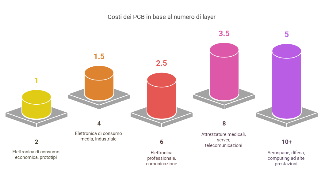
The X multiplier is shown at the top; the number of layers at the bottom.
Total Cost of Ownership (TCO) analysis reveals that the PCB production price is often only a fraction of the overall cost of developing and maintaining an electronic product. A well-designed stackup can significantly reduce the hidden costs associated with:
- Redesigns caused by signal integrity or EMI issues
- Additional testing required to validate non-optimal solutions
- External components (filters, shielding) needed to compensate for stackup shortcomings
- Reduced reliability, and the consequent increase in warranty costs
- Delayed time-to-market due to design iterations
The value of a robust PCB architecture becomes particularly evident in high-reliability sectors such as medical, automotive and aerospace, where the costs of a failure can be orders of magnitude higher than the initial savings obtained from an economical design.
Case Study: Cost-Benefit Analysis in an Industrial Application
Here’s an application case I came across in the literature: an industrial control equipment manufacturer ran a comparative analysis between two design approaches for a new system:
- Option A: 4-layer PCB with additional components for filtering and protection
- Option B: 6-layer PCB with stackup optimized for EMC and signal integrity
Production costs for 10,000 units showed a clear advantage for Option A:
- PCB cost, Option A: €12/unit (total €120,000)
- PCB cost, Option B: €18/unit (total €180,000)
However, the TCO analysis revealed a completely different picture:
Cost item**Option A (4 layers)**Option B (6 layers)PCB€120,000€180,000Additional EMI components€40,000€5,000Additional EMC testing€15,000€5,000Time-to-market delay€70,000€0Estimated warranty costs€35,000€10,000Total**€280,000**€200,000
Setting aside the precision of the estimates, this example illustrates how the apparently cheaper decision can turn out to be more expensive over the product’s full life cycle. Optimizing the stackup represents an investment in the overall quality of the system, with tangible returns in terms of reliability and time-to-market.
One further economic consideration is production scalability. A well-designed stackup makes the transition from low to high production volumes smoother, letting you maintain the same electrical characteristics even when moving from prototype-oriented PCB manufacturers to mass-production ones. This flexibility can be decisive in scenarios of rapid demand growth.
In light of these considerations, the optimal stackup is one that meets the minimum technical requirements with a reasonable safety margin, balancing performance and cost in the context of the product’s entire life cycle.
Implementation Strategies for Different Applications
Consumer Applications
For consumer devices such as smartwatches, tablets and peripherals, the optimal approach tends to use 4-6 layer PCBs in FR4:
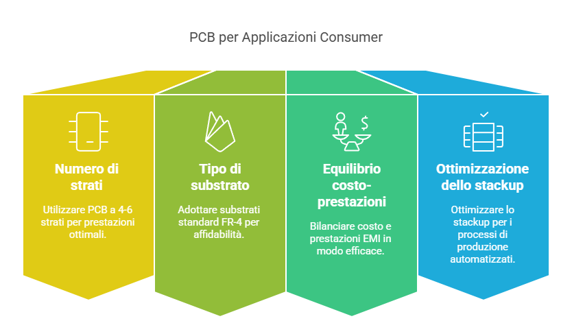
In consumer electronics, balancing cost and performance is critically important. The typically thin margins demand a careful design that optimizes every aspect of the stackup without over-specifying.
An effective approach is to identify the truly critical signals that need impedance control and protection from interference, assigning them privileged positions in the stackup. Less critical signals can be managed with more relaxed specs, reducing production costs.
Stackup symmetry becomes particularly important for thin devices like smartphones and tablets, where even minor deformations can cause assembly or reliability issues. A structure that is symmetrical about the center axis effectively prevents warping, helping to maximize production yield.
Application case: smartwatch with heart-rate monitoring
A smartwatch manufacturer optimized the stackup to balance the conflicting needs of miniaturization, thermal management and signal integrity:
- 6-layer PCB in FR-4 with high glass-transition temperature (Tg 170°C)
- Symmetric stackup with a total thickness of just 0.8 mm
- Dedicated layers to isolate analog circuits (sensors) from digital
- Via-in-pad for fine-pitch BGA components
- Optimized thermal dissipation areas for the processor
This configuration made it possible to:
Reduce the footprint by 20% compared to the previous generation.
Improve battery life through better thermal management.
Maintain heart-rate sensor accuracy despite the proximity of noisy digital circuits.
Respect the budget constraints for a consumer-market product.
Industrial Applications
Industrial electronics demands greater robustness:
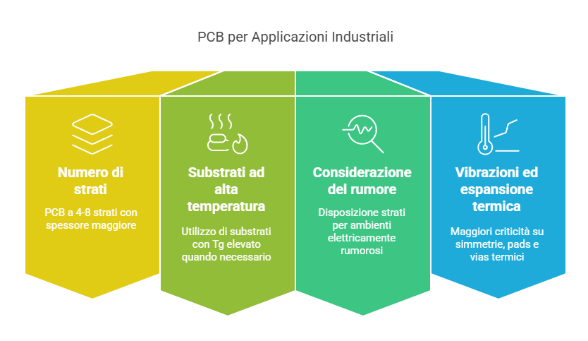
Industrial applications present unique challenges tied to often harsh operating environments. Extreme temperatures, continuous vibrations, humidity and chemical contaminants call for specific considerations in stackup design.
The choice of materials takes on critical importance in this context. Substrates with high glass-transition temperature (Tg) and decomposition temperature (Td) ensure structural stability even in hot environments. For use in particularly aggressive environments, special laminates such as high-Tg FR-4, polyimide or PTFE offer superior chemical and thermal resistance.
The overall thickness of the PCB and the copper tends to be greater than in consumer electronics, increasing mechanical robustness and thermal dissipation capacity. This is particularly important for devices that may be subject to mechanical stress or that dissipate significant power.
EMI protection plays a fundamental role in industrial environments, characterized by strong electromagnetic fields generated by motors, inverters and power equipment. A stackup optimized for these applications typically has multiple ground layers and integrated shielding techniques.
Application case: industrial automation controller
A PLC controller destined for harsh industrial environments implemented a specialized stackup:
- 8-layer PCB with a total thickness of 2.4 mm for mechanical robustness
- 2 oz copper (i.e. 70 μm) on the outer layers to improve thermal dissipation
- High-Tg FR-4 substrate (180°C) to withstand elevated temperatures
- Dedicated internal layers to segregate analog field signals from digital logic
- Multiple ground planes to improve EMI shielding
- Perimeter via stitching to create an integrated “Faraday cage”
This configuration enabled the device to:
- Operate reliably in environments with temperatures from -40°C to +85°C
- Withstand continuous vibrations up to 5G
- Maintain electromagnetic compatibility even near power inverters
- Guarantee an estimated operating life of more than 15 years
High Frequency and RF
Radio-frequency circuits call for specialized considerations:
- Low-loss substrates (Rogers, PTFE)
- Strictly controlled impedance
- A dedicated ground plane for every signal layer
- Minimization of vias and discontinuities
RF applications are among the most complex challenges in stackup design. At high frequencies (typically above 1 GHz), material behavior changes significantly and phenomena that are often negligible at low frequencies become dominant.
The choice of dielectric material is probably the most critical aspect. Traditional FR-4 laminates exhibit significant losses and non-homogeneous properties at high frequencies. Special materials such as Rogers RO4350B, Isola I-Tera, or PTFE (Teflon) offer:
- A dielectric constant that is stable across frequency
- Low dissipation factor (tan δ)
- Superior homogeneity
- Thermal and dimensional stability
Stackups for RF applications typically have a multi-level structure where every signal layer sits next to a dedicated ground plane. This configuration minimizes interference and makes impedance control easier.
Transitions between different propagation structures are a critical point. Every discontinuity (via, width change, bend) introduces reflections that can significantly degrade performance. An optimal design minimizes these transitions and tunes them through electromagnetic simulations.
Application case: 5G mmWave module
A communication module operating in the 28 GHz millimeter band required a highly specialized stackup:
- 8-layer PCB with Rogers RO4350B material (εr = 3.48, tan δ = 0.0037)
 Dielectric thicknesses tuned to obtain controlled impedance for CPWG (Coplanar Waveguide with Ground) lines
- Surface layers dedicated to RF circuits with ultra-smooth copper to reduce losses
- Optimized transitions between components and transmission lines
- Embedded resonant structures for filtering
- Via fences to isolate the critical RF paths
The design required extensive 3D electromagnetic simulation to optimize:
- Insertion losses (< 0.5 dB on critical interconnects)
- Channel coupling (< -25 dB in the operating band)
- Impedance stability (50 Ω ±3% on all lines)
This meticulous attention to the stackup made it possible to achieve excellent performance in a compact form factor, essential for integration into mobile devices.
Automotive and Aerospace
For safety-critical applications:
- Redundant stackups with 8+ layers
- Physical separation between critical circuits
- Materials with controlled thermal expansion coefficient
- Compliance with sector-specific standards
The automotive and aerospace sectors impose particularly strict requirements for reliability and safety. The reference standards (ISO 26262 for automotive, DO-254 for avionics) require systematic approaches to risk mitigation, with direct impacts on stackup design.
A distinctive aspect of these applications is the wide operating temperature range, which can go from -55°C to +125°C or beyond. This thermal range calls for specific considerations around dimensional stability and compatibility between the coefficients of thermal expansion (CTE) of the different materials.
Redundancy is a fundamental principle for critical systems. At the stackup level, this translates to:
- Duplication of critical connections on different layers
- Physical separation between redundant circuits
- Galvanic isolation between functional domains
- Advanced protection against electrostatic discharge and transients
Stackups for these applications tend to be more conservative in terms of density and design margins. Routing rules are typically stricter, with greater isolation distances and wider paths for higher currents.
Application case: ADAS control unit
 A control unit for ADAS (Advanced Driver Assistance Systems) implemented a sophisticated stackup to ensure reliability and safety:
- 10-layer PCB with automotive-qualified IPC-4101/126 material
- 1 oz copper (35 μm thick) for internal layers and 2 oz (70 μm) for external layers
- Duplicated signal layers for critical connections with independent routing
- Complete segregation between power, signal and sensor circuits
- Galvanic isolation zones between functional domains implemented with slots in the PCB
- Separate ground planes for analog and digital circuits with a controlled connection point
The configuration underwent rigorous testing:
- Thermal cycling (-40°C/+125°C, 1000 cycles)
- Vibration testing (5-2000 Hz, 30G)
- Advanced EMC testing to CISPR 25 Class 5 standard
- Failure analysis using FMEA methodology
This approach made it possible to develop a system that meets ASIL-D (Automotive Safety Integrity Level D) requirements — the highest level specified by the ISO 26262 standard — ensuring the functional safety needed for autonomous driving applications.
Practical Guidelines for Choosing a Stackup
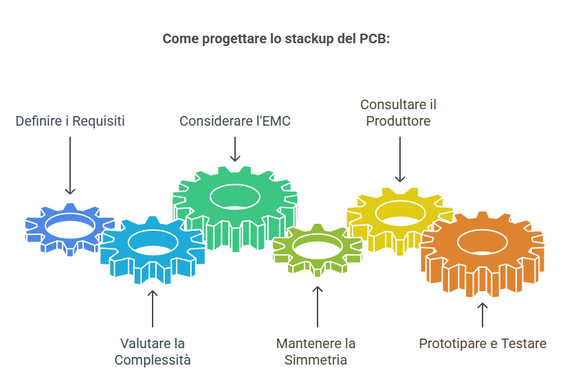
- Define the requirements: clarify operating frequencies, component density, thermal constraints
- Assess the complexity: estimate the number of connections and the routing density
- Consider EMC: identify noise sources and sensitive circuits
- Keep it symmetric: balance the stackup around the center axis
- Consult the manufacturer: check manufacturing capabilities and costs
- Prototype and test: validate the stackup with EMC and thermal testing
Defining the requirements is the fundamental starting point for designing an effective stackup. This phase should include a clear identification of:
- Electrical specifications (frequencies, interfaces, impedances)
- Mechanical constraints (dimensions, thickness, stiffness)
- Environmental requirements (temperature, humidity, vibration)
- Reliability expectations (MTBF, operating life)
- Cost and production constraints (volumes, available technologies)
A careful assessment of circuit complexity helps determine the minimum number of layers needed. Estimation techniques such as calculating interconnect density (connections per square inch) or analyzing the fanout of critical components provide useful quantitative guidance for this decision.
Preliminary EMC analysis should identify potential electromagnetic compatibility issues before the stackup is finalized. Separating sensitive circuits from noisy ones, both horizontally and vertically through the stackup, is an effective preventive strategy.
Early consultation with PCB manufacturers is essential to ensure the feasibility of the proposed stackup. Special materials, non-standard thicknesses or particular impedance requirements must be verified with the supplier before the design is finalized.
Stackup for a New Product: A Structured Decision Process
A methodical approach to defining the stackup might follow this flow:
-
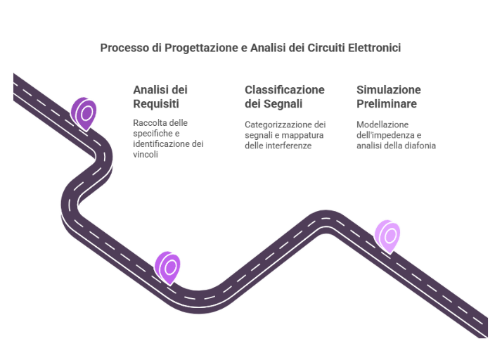 Requirements analysis
Collecting electrical, mechanical and environmental specifications
Requirements analysis
Collecting electrical, mechanical and environmental specifications -
Identifying critical components (BGA, RF, high-speed)
-
Defining production and cost constraints
-
Signal classification Categorization by criticality (high-speed, sensitive analog, power)
-
Mapping of potential interference
-
Defining separation rules
-
Preliminary simulation Impedance modeling for various configurations
-
Crosstalk analysis for critical pairs
-
Signal-loss evaluation
-
Initial stackup definition Selecting the number of layers and their function
-
Defining geometries for controlled impedance
-
Preliminary mapping of power domains
-
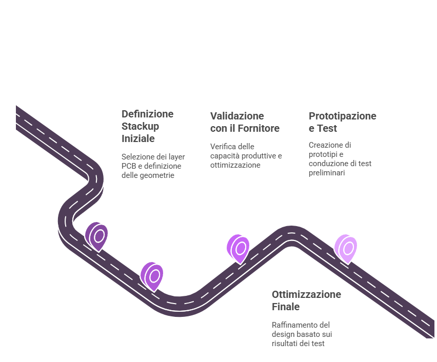 Validation with the manufacturer
Verification of production capabilities
Validation with the manufacturer
Verification of production capabilities -
Adaptation to the supplier’s design rules
-
Optimization for manufacturability
-
Prototyping and testing Fabrication of prototypes with test coupons
-
Validation of the actual impedance
-
Preliminary EMC tests
-
Final optimization Refinement based on test results
-
Implementation of incremental improvements
-
Full documentation of the specifications
This iterative process lets you converge on an optimal stackup that balances performance, manufacturability and cost.
Future Trends in Layer Arrangement
Technology is driving toward:
- Advanced materials: substrates with better thermal and electrical properties
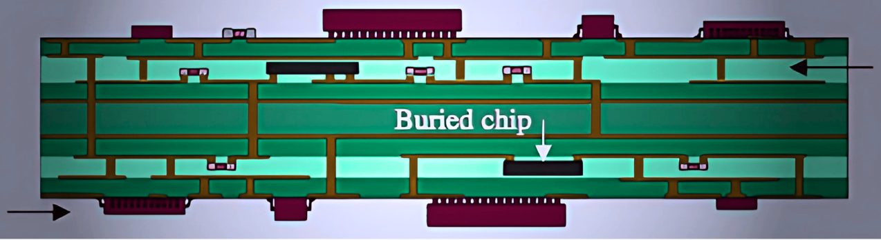
- Embedded technologies: components integrated within the stackup itself
- Multi-layer flexible PCBs: complex stackups on flexible substrates
- 2.5D and 3D integration: high-density vertical interconnects
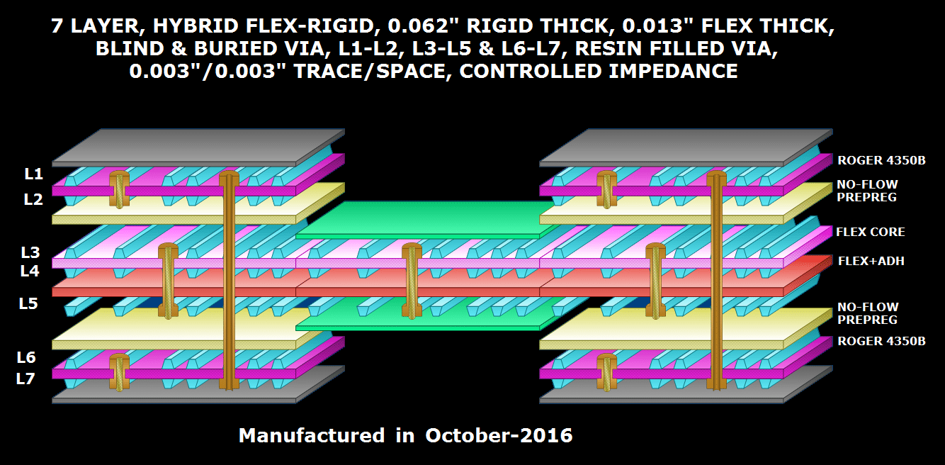
- Hybrid stackups: combining different technologies within the same PCB
These trends call for ever more sophisticated approaches to stackup design, with growing integration between electrical, thermal and mechanical design.
PCB material evolution is proceeding in several complementary directions. One significant trend is the development of laminates with better thermal properties, essential for managing the growing power density of modern devices. Ceramic materials and metal-ceramic composites offer thermal conductivities up to 10 times higher than traditional FR-4, enabling efficient dissipation without increasing PCB thickness.
In parallel, high-performance RF materials are becoming more accessible. Laminates once reserved for military or space applications are finding their way into consumer products, thanks to the spread of high-frequency communications (5G, WiFi 6E, automotive radar). These materials offer low dielectric losses and dielectric constants that remain stable up to frequencies of tens of GHz.
Embedded component technology represents one of the most promising innovations. Passive components (resistors, capacitors) and even active ones (silicon dies) are integrated directly inside the laminate, creating three-dimensional structures that optimize space and performance. This technology requires highly specialized stackups with cavities and precise vertical connections.
Emerging example: PCBs with integrated passive components
A recent wearable electronics product implemented an innovative stackup with integrated passive components:
-
10-layer PCB with a total thickness of just 0.6 mm
-
Array of 0201 capacitors and 0402 resistors embedded between layers 4 and 5
-
Blind-via and microvia technology for high-density vertical connections
-
40% surface-area reduction compared to the traditional design
-
30% improvement in RF performance thanks to fewer discontinuities
2.5D and 3D integration represents the next horizon in stackup evolution. Technologies such as silicon interposers, package-on-package and through-silicon vias (TSVs) are redefining the boundary between PCB and component packaging. These solutions require stackups with precisely controlled electrical, thermal and mechanical properties, able to interface with the microscopic structures of modern packages.
Hybrid stackups, which combine different materials and technologies in a single PCB, are emerging as a solution for multi-function devices. One example is PCBs that integrate rigid and flexible sections, or that combine high-performance RF areas with zones optimized for power or digital signals.
Conclusion
Stackup design is a fundamental architectural decision that influences the entire life cycle of an electronic product. An optimal layer arrangement balances electrical, thermal, mechanical and economic requirements, offering a competitive advantage in terms of performance, reliability and time-to-market.
The stackup isn’t just a technical aspect of design, but a strategic decision that defines the fundamental capabilities and limits of an electronic system. The increasing complexity of modern devices, integrating different technologies (digital, analog, RF, power) into ever smaller spaces, makes this architectural decision even more critical.
 The optimal approach to stackup design requires a holistic view that integrates different perspectives: the electrical needs of signal integrity and electromagnetic compatibility, the thermal requirements for efficient heat dissipation, the mechanical constraints for strength and stability, and the economic considerations related to cost and manufacturability.
For designers, it’s essential to consider the stackup in the earliest stages of the development process, collaborating closely with PCB manufacturers to ensure feasibility and cost optimization. For decision-makers, understanding the impact of the stackup on the final product’s performance allows for appropriate resource allocation and realistic specifications.
The fundamental principles presented in this article — symmetry, appropriate segmentation, impedance control, and optimal signal distribution — provide a solid basis for tackling this design challenge. However, every application presents unique characteristics that require specific considerations and, often, carefully weighed trade-offs.
In a continuously evolving technological context, the ability to design optimized stackups becomes a strategic skill that differentiates excellent products from mediocre ones. Companies that invest in this competence can achieve significant advantages in terms of quality, cost and development speed.
Emerging trends in materials and interconnect technologies promise to further expand the possibilities, enabling ever higher performance in ever smaller spaces. Designers who thoroughly understand the fundamental principles of stackup design will be better equipped to leverage these innovations and develop the next generation of electronic products.