

Analog to Digital – SAR, Flash and Hybrid Converters: High-Efficiency, High-Speed Architectures
Analog to Digital – SAR, Flash and Hybrid Converters: High-Efficiency, High-Speed Architectures

Lorenzo Martini, 15/06/2026
Introduction: Two Divergent Approaches to Analog-to-Digital Conversion
In the broad landscape of analog-to-digital conversion technologies, SAR (Successive Approximation Register) and Flash architectures represent two profoundly different — almost opposing — philosophies, each answering specific application needs. On one hand, the SAR converter embodies a sequential, efficient approach, optimizing hardware resource use through an iterative algorithm. On the other, the Flash converter is the “brute force” solution, favoring absolute speed through massive parallelization.
These two architectures dominate complementary market segments, and a deep understanding of both is essential for designers and decision-makers tasked with selecting the most appropriate conversion technology for a given application. In today’s context, shaped by the growing importance of real-time signal processing and the expansion of the Internet of Things (IoT), these architectures have taken on an even more strategic role in the modern electronics ecosystem.
In this article we explore, in detail, the operating principles, performance parameters, advantages and limits of both architectures, providing a comparative framework that highlights each one’s optimal application domains.
Successive Approximation (SAR) Converters: The Binary Algorithm in the Service of Efficiency
The SAR converter implements a binary search algorithm to determine, bit by bit, the digital representation that best approximates the analog input value. Much like a guessing game where each question halves the search space, the SAR converter progressively narrows down the uncertainty on the analog value.
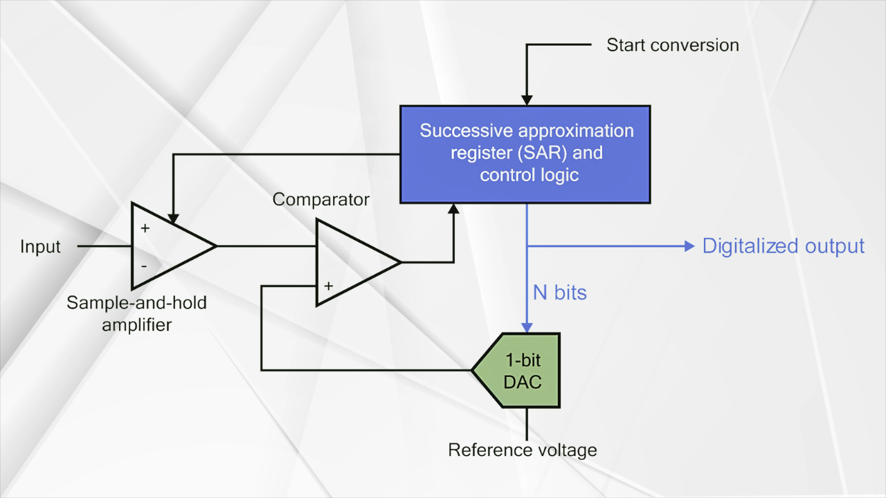
The basic architecture of a SAR ADC comprises four fundamental elements:
- Sample-and-Hold circuit: samples and holds the analog signal steady throughout the conversion process.
- Comparator: compares the analog signal with the internal DAC output.
- SAR register: stores the progressive conversion result and implements the approximation algorithm logic.
- Digital-to-Analog Converter (DAC): converts the current digital value into an analog signal for comparison, progressively reducing the uncertainty on the analog value.
Conversion Algorithm
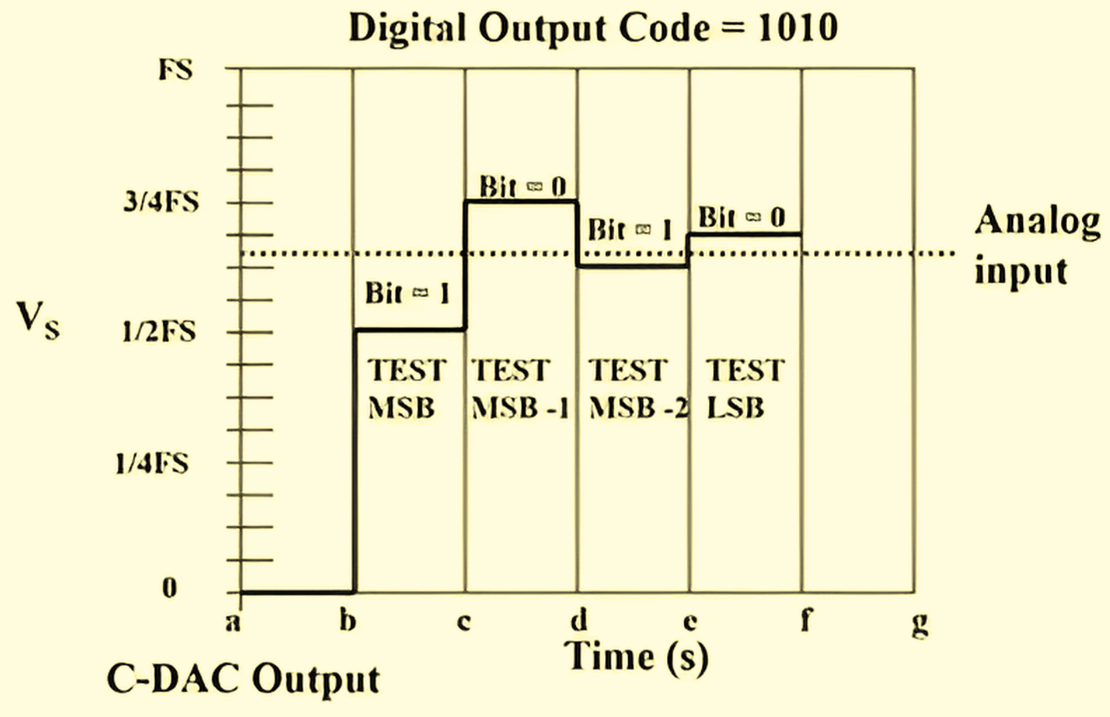
The SAR algorithm operates as a well-defined sequence:
-
The sample-and-hold circuit captures and locks the analog input value (Vin).
-
The SAR register is initialized with the most significant bit (MSB) set to 1 and all others to 0.
-
The current register value is fed to the DAC, which produces a corresponding analog signal (VDAC).
-
The comparator compares VDAC with Vin: If VDAC > Vin, the current bit is cleared
-
If VDAC ≤ Vin, the current bit stays at 1
-
The algorithm moves to the next bit, setting it to 1.
-
Steps 3-5 are repeated until the least significant bit (LSB) is processed.
-
At the end, the SAR register holds the digital representation of the analog value.
This process takes exactly N clock cycles for an N-bit converter, regardless of the input value.
Advanced Implementations
Modern SAR ADC implementations incorporate numerous refinements over the basic architecture, significantly improving performance:
Switched-Capacitor DAC: replaces the traditional resistor DAC with a capacitor network, offering advantages in accuracy, power consumption and area. This implementation leverages the precision of capacitive matching in modern CMOS processes.
Digital Calibration Techniques: compensate for component mismatch errors, improving parameters such as INL, DNL and offset. These techniques can be implemented either at the factory or dynamically during operation.
Split-Capacitor Architectures: reduce DAC area and power by splitting the capacitor network into sections, with an exponential reduction in total required capacitance.
Differential Sampling: improves immunity to noise and interference by using differential rather than single-ended inputs.
Performance and Limitations
SAR converters strike an excellent balance between several performance parameters:
Resolution: typically between 8 and 16 bits, with advanced implementations reaching 18-20 bits.
Speed: from a few hundred kSPS up to tens of MSPS in the fastest implementations. The sequential nature of the algorithm imposes an intrinsic limit on maximum speed.
Power Consumption: generally very efficient, with figures of merit (FoM) that can reach a few femtojoules per conversion — ideal for low-power applications.
Accuracy: good linearity and low distortion, particularly in advanced implementations with calibration techniques.
Silicon Area: relatively compact, growing linearly (rather than exponentially) with resolution.
The main limitation of the SAR architecture is the maximum conversion speed, bounded by the number of clock cycles required to complete the algorithm.
Application Case: Multi-Parameter Biomedical Monitoring System
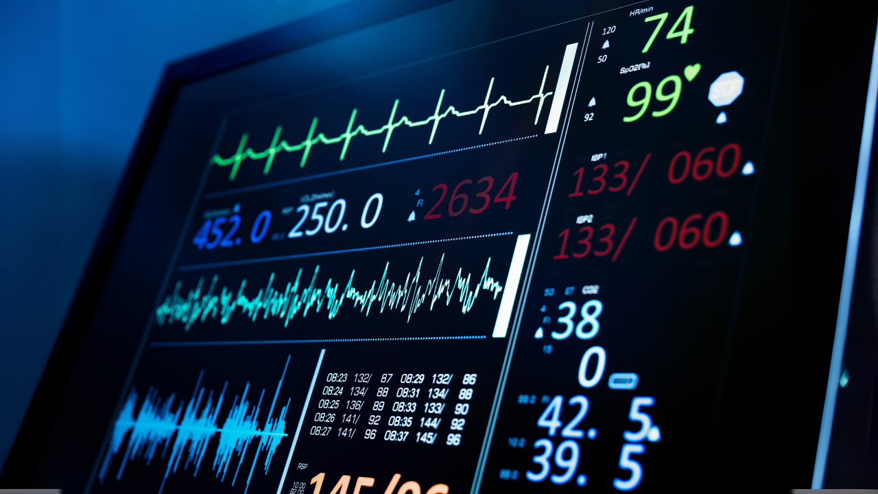
A concrete example of an ideal SAR application is a multi-parameter monitoring system for biomedical use.
Scenario: a wearable device for continuous monitoring of vital signs (ECG, body temperature, oximetry, blood pressure) must operate at low power for long battery life, while maintaining enough precision to ensure diagnostic reliability.
Implementation:
- 12-bit SAR converter with configurable sampling rate (250 SPS – 2 kSPS)
- Analog front-end with programmable-gain amplifier to accommodate different signals
- Analog multiplexer to handle up to 8 input channels
 Power-saving modes with automatic wake-up on events
Performance:
- Power consumption: 30 μW per channel at 1 kSPS
- Effective resolution (ENOB): 11.2 bits
- Conversion time: 8 μs per sample
- Reference voltage: internal (1.25V) with thermal stability < 10 ppm/°C
This solution allows continuous vital-sign monitoring with more than a week of autonomy using a small lithium battery, while retaining the accuracy needed to identify clinically significant anomalies.
Flash Converters: The Architecture of Maximum Speed
The Flash (or parallel) converter represents the most direct approach to analog-to-digital conversion, simultaneously performing all the comparisons needed to determine the final digital code.
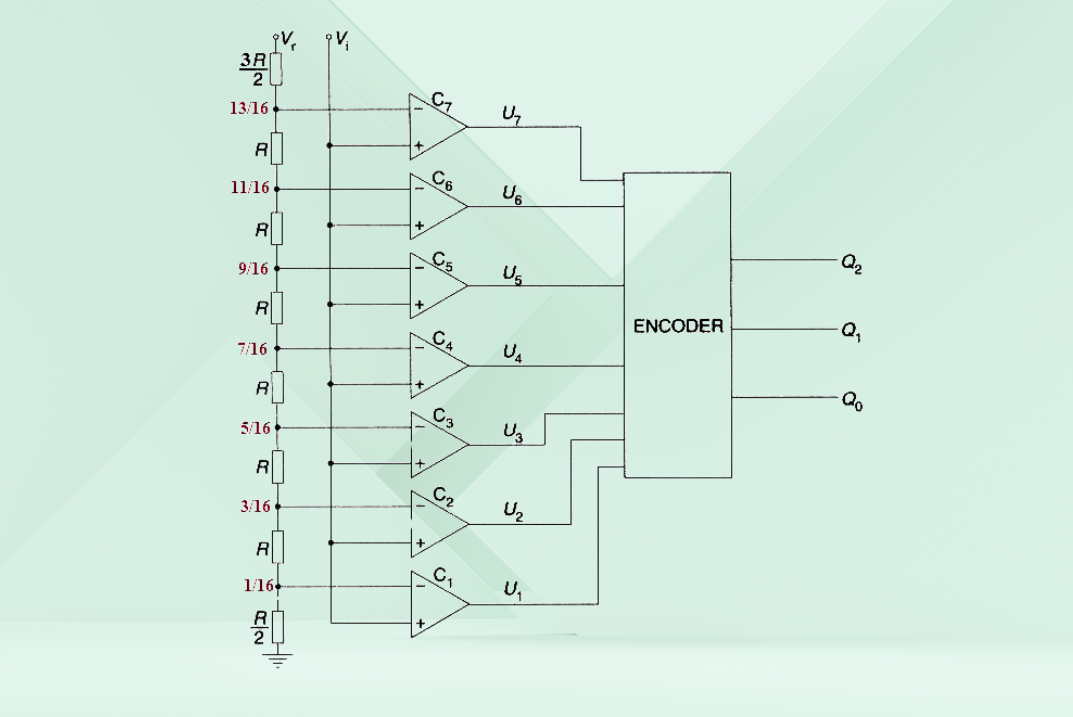
The basic architecture of a Flash ADC includes three fundamental elements:
- Reference Resistor Network: generates 2N-1 reference voltage levels uniformly distributed between the minimum and maximum of the full scale.
- Comparator Array: each comparator simultaneously compares the input signal to one of the reference levels.
- Priority Encoder: converts the comparator output pattern into the final binary format.
Conversion Process
The conversion process in a Flash ADC is conceptually simple and direct:
-
The analog input signal is applied simultaneously to all comparators.
-
Each comparator produces a binary output based on the comparison against its reference level: If Vin > Vref(i), the output is 1
-
If Vin ≤ Vref(i), the output is 0
-
The comparator outputs form a “thermometer code” in which all comparators up to a certain point return 1, and all subsequent ones return 0.
-
The priority encoder converts the thermometer code into the corresponding binary representation.
The entire conversion essentially happens in a single clock cycle, limited only by propagation delays through the comparators and the encoder.
Advanced Implementations
Modern Flash ADC implementations incorporate numerous optimizations to improve performance and mitigate intrinsic issues:
Interpolation Architectures: reduce the number of physical comparators using interpolation techniques between adjacent nodes, significantly lowering area and power.
Averaging and Folding Techniques: further reduce hardware complexity while keeping performance comparable.
Dynamic Calibration: compensates for comparator offset variations that can cause monotonicity and linearity errors.
Differential Architectures: improve noise and common-mode rejection.
Performance and Limitations
Flash converters deliver unmatched speed, but with significant trade-offs:
Speed: extremely high — from hundreds of MSPS up to several GSPS in the most advanced implementations — making this architecture unbeatable for very-high-frequency applications.
Resolution: typically limited to 8 bits or less, with rare implementations reaching 10 bits at the cost of substantial complexity.
Power Consumption: very high, with figures of merit (FoM) generally in the pJ/conversion range or above, limiting applicability in low-power systems.
Silicon Area: grows exponentially with resolution, making high-resolution implementations impractical. An 8-bit Flash ADC needs 255 comparators, while a 10-bit version requires 1023.
Layout Complexity: the large number of identical comparators demands careful layout to ensure uniform performance and minimize systematic errors.
The main limitations of the Flash architecture are high power consumption, silicon area that grows exponentially with resolution, and the implementation challenges of keeping all comparators uniform in behavior.
Application Case: Digital Receiver for High-Speed Optical Communications
An emblematic example of an ideal Flash application is a digital receiver for optical communication systems.
Scenario: a 100 Gbps optical communication system using PAM-4 modulation (4-level Pulse Amplitude Modulation) requires a receiver capable of sampling the signal at 50+ GSample/s with enough resolution to discriminate the four amplitude levels.
Implementation:
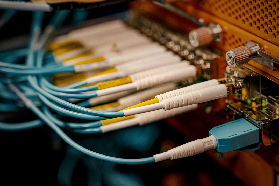
- 6-bit Flash converter with 56 GSPS sampling rate
- Analog front-end with ultra-wideband amplifier (>25 GHz)
- Adaptive equalizer implemented digitally post-conversion
- Advanced process technology (28 nm or below) to handle the clock frequencies
Performance:
- Analog bandwidth: >28 GHz
- ENOB at Nyquist: 4.8 bits (sufficient for PAM-4 modulation)
- Power: 1.8W (acceptable for this high-performance application)
- Aperture jitter: <150 fs RMS
This solution enables a fully digital receiver for optical communication systems, pushing most of the signal processing into the digital domain and increasing system flexibility through programmable processing techniques.
Comparative Analysis: When to Choose SAR vs Flash
The choice between SAR and Flash architectures must be grounded in a careful analysis of application requirements and the associated trade-offs. The following table offers a direct comparison of the main characteristics:
Parameter**SAR ADC**Flash ADCSpeedMedium (up to ~20 MSPS)Very high (up to GSPS)ResolutionHigh (8-16 bits, up to 20)Low (typically 4-8 bits)Power consumptionLow (fJ/conversion)High (pJ/conversion)Silicon areaModerate, grows linearlyLarge, grows exponentiallyCircuit complexityMediumHighLatencyMedium (N cycles for N bits)Very low (single-stage pipeline)Thermal driftModerateSignificantNoise immunityGoodModerate
Optimal Application Domain: SAR
SAR converters are the ideal choice when:
-
Energy efficiency is a priority Battery-powered devices
-
Energy harvesting systems
-
Wireless sensor networks
-
Resolution matters more than speed Precision instrumentation
-
Multi-channel data acquisition
-
Industrial control systems
-
Silicon resources are limited Low-cost embedded systems
-
High-density-integration IoT applications
-
Wearable devices
Example application: a distributed environmental monitoring system with hundreds of battery-powered nodes needs energy-efficient converters. Implementation with 12-bit SAR ADCs operating at 10 kSPS provides sufficient resolution for environmental measurements (temperature, humidity, air quality) at under 50 μW per channel. This enables sensor nodes with years of autonomy using standard batteries or energy-harvesting techniques.
Optimal Application Domain: Flash
Flash converters are the optimal choice when:
-
Speed is the critical parameter Digital oscilloscopes
-
Radar and defense systems
-
High-speed digital communications
-
Latency must be minimal Closed-loop control systems
-
Real-time spectrum analyzers
-
High-speed trigger systems
-
Power consumption is not a primary constraint Laboratory equipment
-
Network infrastructure
-
Mains-powered systems
Example application: an automotive radar system requires processing of reflected RF signals with minimal latency to identify obstacles and fast-moving vehicles. An 8-bit Flash ADC operating at 1 GSPS allows direct digitization of the IF signal after the mixer, enabling advanced processing algorithms in an FPGA or DSP. The low latency of the Flash ADC is crucial for ensuring adequate response times in safety-critical scenarios such as automatic emergency braking.
Hybrid Architectures: The Best of Both Worlds
The intrinsic limitations of pure architectures have led to the development of hybrid approaches that combine elements of different topologies to achieve more favorable performance trade-offs.
[FIGURE 16: Block diagrams of hybrid architectures, in particular: (a) two-stage Flash ADC, (b) Half-Flash ADC, and (c) Folding ADC, highlighting the advantages over pure architectures]
Two-Stage Flash ADC
This architecture splits the conversion into two steps, using two low-resolution Flash converters in cascade:
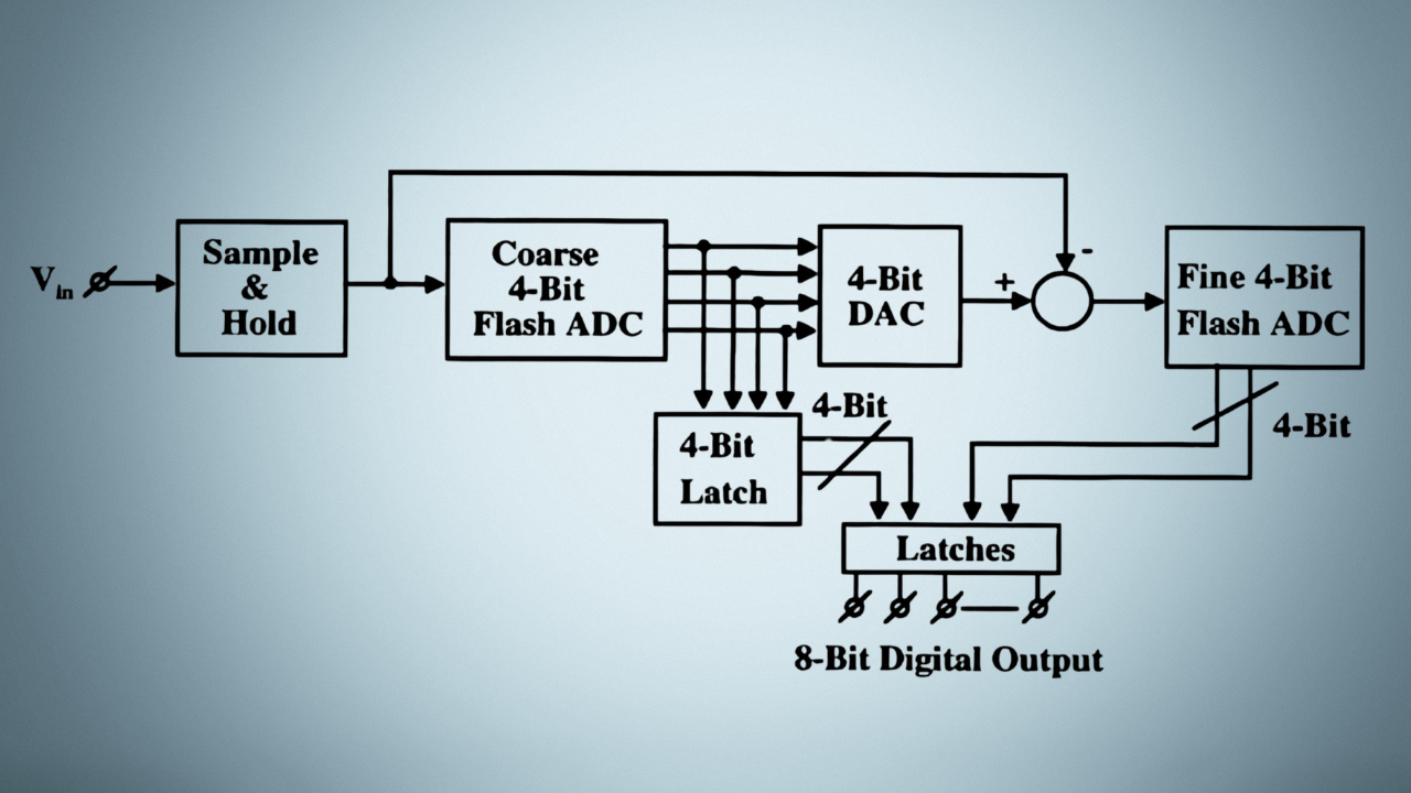
- The first stage resolves the most significant bits
- A DAC reconstructs the corresponding analog value
- A residue amplifier computes the difference between the original input and the reconstructed value
- The second stage converts the least significant bits from the residue signal
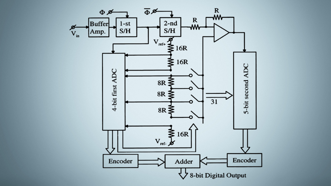 This approach drastically reduces the number of comparators needed. For instance, an 8-bit ADC can be implemented with two 4-bit stages, requiring only 30 comparators instead of 255.
Half-Flash ADC
This architecture, also known as “Two-Step Flash”, uses a single comparator array in two successive cycles:
- In the first cycle, the converter determines the most significant bits
- Based on the result, the comparator references are reconfigured
- In the second cycle, the least significant bits are determined
This approach halves the number of comparators needed at the cost of reduced speed.
Folding ADC
The folding architecture is an evolution of the Flash approach that significantly reduces hardware complexity:
- “Folder” circuits fold the input signal, reusing the same comparators for different intervals of the full scale
- The number of comparators goes from exponential to linear with resolution
- Most of the speed advantage of the Flash architecture is preserved
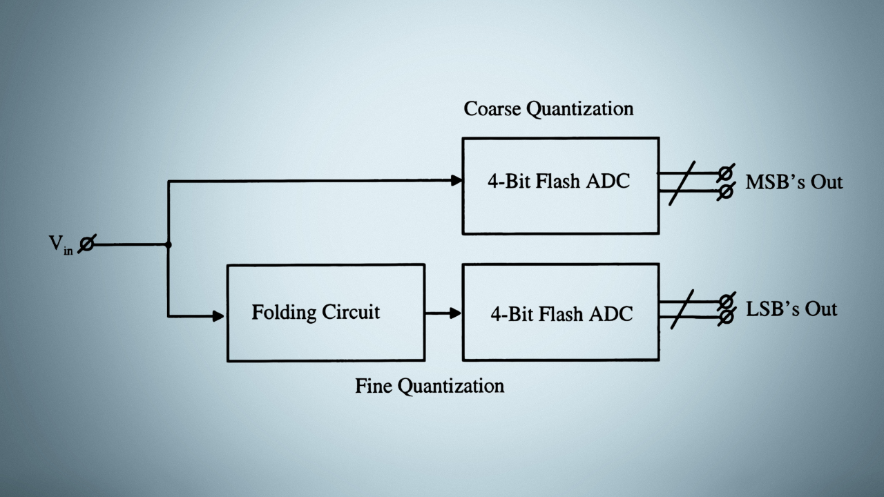
This technique is particularly effective for medium-resolution (8-10 bits), high-speed converters.
Application Case: Software-Defined Radio Receiver with Folding ADC
A concrete example of a hybrid architecture is a Software-Defined Radio (SDR) receiver for military or advanced telecommunication applications.
Scenario: a military SDR system must cover a wide frequency range (from a few MHz to 6 GHz) with several modulation modes, requiring high dynamic range and good resolution at considerable speeds.
Implementation:
- 10-bit folding-interpolating converter with 250 MSPS sampling rate
- RF front-end with direct or low-IF conversion for the bands of interest
- High-performance FPGA for real-time data-stream processing
- Dynamic calibration system to correct the converter’s non-idealities**
 **
**
Performance:
- Analog bandwidth: >500 MHz
- ENOB: 8.7 bits at 100 MHz IF
- SFDR: >65 dB
- Power: 350 mW
This hybrid solution delivers an excellent compromise between speed, resolution and power, making it possible to build a flexible receiver that adapts to different waveforms and operating conditions — a key requirement for advanced SDR applications.
Technology Evolution and Future Trends
Over the last twenty years, both architectures have benefited from significant technological advances:
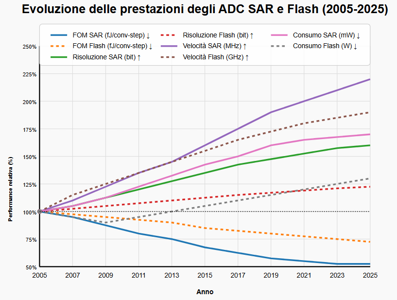
For SAR converters:
- Adoption of asynchronous sampling techniques to improve energy efficiency
- Development of time-domain architectures that convert voltage into timing to improve scalability with nanometer processes
- Background calibration techniques to compensate for DAC non-idealities
- Variable-resolution architectures that dynamically trade off precision and power
For Flash converters:
- Regenerative-feedback comparators with drastically lower power
- New digital encoder topologies resistant to bubble errors
- Digital calibration techniques to compensate for process variations
- Integration of low-noise preamplifiers to improve effective resolution
Future Trends
Process-technology evolution and emerging application needs are driving several significant trends:
- System Integration: increasing integration of ADCs into complex SoCs, with optimization of the entire data acquisition and processing chain.
- Optimization for Nanometer Technologies: architectures are being adapted to exploit the advantages of nanometer processes, favoring time-domain rather than voltage-domain solutions.
- Application Specialization: architectures tailored for specific domains such as IoT, edge computing, automotive and 5G/6G.
- Machine-Learning Techniques: ML algorithms for adaptive calibration and error compensation, improving dynamic performance.
Technology Roadmap
Over the next 3-5 years we can anticipate:
- SAR ADCs with figures of merit below 1 fJ/conversion, enabling new ultra-low-power applications.
- Flash converters with extended resolution (10+ bits) while maintaining GSPS speeds, thanks to advanced calibration techniques.
- Tighter integration of pre- and post-processing functions directly within the converters.
- Reconfigurable architectures that dynamically adapt to different operating scenarios.
Economic and Market Considerations
Having covered the technical aspects of these devices, it’s equally important to look at other parameters that have a major influence on their usability — namely the cost and availability of the various solutions:
SAR ADCs:
- Price range: from under $1 for basic versions up to $20-50 for high-performance implementations.
- Availability: broad product range from many suppliers.
- Implementation cost: relatively low, with good scalability.
Flash ADCs:
- Price range: from $5-10 for simple versions up to $100-500 for ultra-high-speed solutions.
- Availability: limited options, especially for the highest-speed versions.
- Implementation cost: high, with significant power and cooling requirements.
Cost-Performance Trade-off
Selecting the optimal converter requires a total-cost-of-ownership (TCO) evaluation:
- Direct component cost: generally more favorable for SAR solutions at equal resolution.
- Energy cost: significantly lower for SAR, with impact on power-supply sizing and thermal management.
- Development cost: potentially higher for Flash solutions, which demand particular attention to routing, signal integrity and EMI management.
- Opportunity cost: to be weighed against overall system performance and the resulting competitive advantages.
Case in point: in an industrial data-acquisition system, the choice between a 16-bit/1 MSPS SAR ADC ($12) and an 8-bit/500 MSPS Flash ADC ($35) must consider not only the technical specs but the product’s entire life cycle. If the application only needs 500 kSPS at 14 bits of resolution, the SAR solution offers a significant economic advantage, not only in component cost but also in a simpler power supply and lower thermal-management requirements.
Conclusion: A Guide to Selecting the Optimal Architecture
The choice between SAR and Flash converters is a classic example of engineering as the art of trade-offs. There’s no universally superior solution, but rather an architecture best suited to each specific application context.
Decision Flowchart
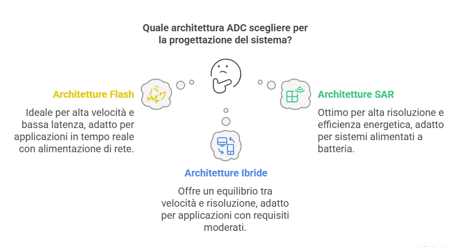
The following decision process can guide the initial selection:
-
Determine the required sampling rate: If > 100 MSPS, lean toward Flash or hybrid architectures
-
If < 20 MSPS, SAR architectures generally offer the best compromise
-
Evaluate resolution requirements: If > 12 bits, SAR architectures are practically mandatory
-
If < 8 bits, consider Flash for speed advantages
-
Analyze energy constraints: With battery or energy-harvesting power, favor SAR
-
With mains power and available cooling, Flash can be acceptable
-
Consider latency requirements: For real-time control systems, the reduced delay of Flash architectures can be decisive
Final Considerations
In the ever-evolving landscape of conversion technologies, it’s essential to:
- Stay up to date on the latest innovations, which can shift traditional trade-offs between architectures.
- Carefully evaluate the entire system, not just isolated converter specifications.
- Consider hybrid implementations that may offer the best compromise for specific applications.
- Empirically verify performance under real operating conditions, not just based on theoretical specifications.
SAR and Flash architectures will continue to coexist, evolving to adapt to new application domains and process technologies. A deep understanding of their strengths and limitations remains an essential tool for engineers and project managers in modern electronics.
In the next article in the series, we’ll explore the advanced Sigma-Delta and Pipeline architectures, which complete the picture of the main ADC topologies and offer additional options for specific applications where neither SAR nor Flash is the optimal fit. See you soon!