

Analog to Digital – Fundamentals and Conversion Principles
Analog to Digital – Fundamentals and Conversion Principles
Lorenzo Martini, 16/03/2026
The Conversion Process: From Physical Quantity to Digital Data
The Conversion Flow
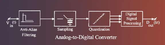
Turning an analog signal into a digital format is not an instantaneous process but a sequence of operations that preserve the integrity and accuracy of the information. Understanding these steps is essential to appreciate the complexities and trade-offs intrinsic to conversion.
The process can be broken down into the following stages:
- Signal conditioning: the analog signal is prepared for conversion through amplification, attenuation, filtering and linearization.
- Sampling: the continuous signal is captured at discrete time intervals, producing a sequence of samples.
- Holding: the sampled value is “frozen” for the time needed to perform the conversion.
- Quantization: the analog value is approximated to the nearest discrete level on the available digital scale.
- Encoding: the quantized value is translated into a binary representation.
The Nyquist-Shannon Sampling Theorem
At the heart of analog-to-digital conversion theory lies a fundamental mathematical principle: the Nyquist-Shannon Sampling Theorem. This theorem states that, in order to faithfully reconstruct a band-limited analog signal, the sampling rate must be at least twice the highest frequency present in the signal.
Formally:
fsample ≥ 2 * fmax
Where:
- fsample is the sampling rate
- fmax is the highest frequency present in the analog signal
This relationship imposes a fundamental constraint on the design of conversion systems. Violating this principle leads to aliasing, where high-frequency components are incorrectly represented as lower frequencies, introducing irreversible distortion in the reconstructed signal.
Quantization and Intrinsic Error
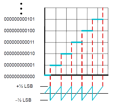
Quantization is an inherent source of error in the conversion process. When a continuous analog value is approximated to one of the available discrete levels, an uncertainty is inevitably introduced — the quantization error.
The maximum amplitude of this error is equal to half the quantization step (LSB, Least Significant Bit), which corresponds to the smallest change the converter can represent. Statistically, assuming a uniform input-signal distribution, the quantization error behaves as additive noise with a uniform distribution over the interval ±½ LSB.
The signal-to-noise ratio arising from this error is directly proportional to the converter’s resolution and can be approximated by the formula:
SNR ≈ 6.02 · N + 1.76 dB
Where N is the number of bits of the converter.
Main ADC Architectures
Different applications call for specific trade-offs between speed, precision, power consumption and cost. This has led to the development of several ADC architectures, each with distinctive characteristics that make it optimal for specific applications.
Successive-Approximation (SAR) ADC
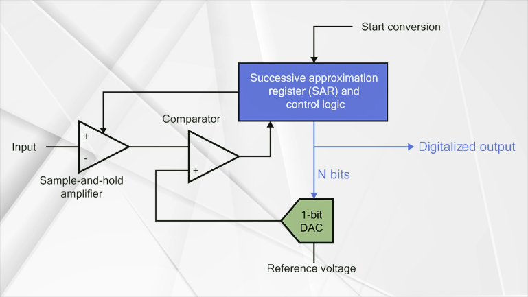
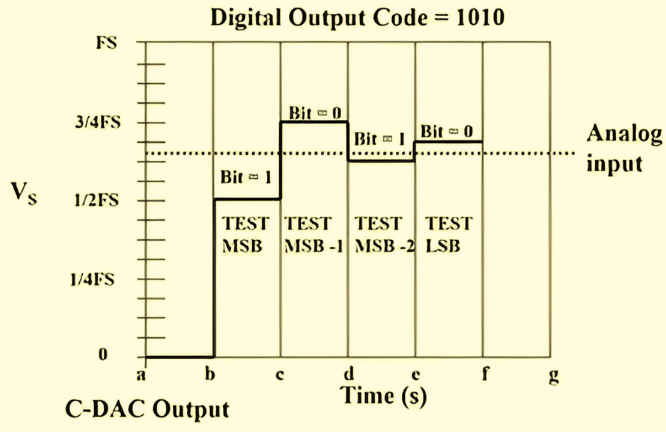
The SAR architecture implements a binary search algorithm to determine the digital value that best approximates the analog input. The process starts at the most significant bit (MSB) and proceeds sequentially toward the least significant bit (LSB).
 **
**  **
**
Operating principle:
- Initialize the SAR register with the MSB set to 1 and all others to 0
- Convert the current digital value to analog via a DAC
- Compare with the input signal
- If the DAC value is greater than the input, clear the current bit
- Move to the next bit, setting it to 1
- Repeat steps 2-5 until the last bit
This architecture offers a good balance between speed, precision and power consumption, with conversion times proportional to the bit resolution.
Application case: an industrial vibration-analysis data-acquisition system needs moderate resolution (12-16 bits) with conversion rates of tens or hundreds of kilosamples per second. The SAR ADC is the ideal fit here, offering a good compromise between precision and speed while keeping power consumption contained. In practice, the implementation uses an analog front-end with anti-aliasing filters configured to limit the signal bandwidth to 40 kHz, followed by a 16-bit SAR converter sampling at 100 kSPS. This allows accurate analysis of vibration phenomena up to 50 kHz, covering most industrial monitoring applications.
Flash (Parallel) ADC
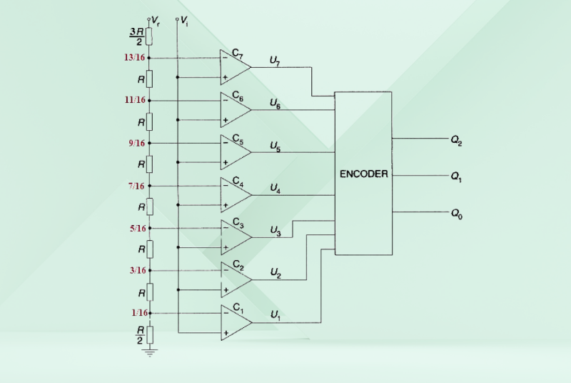
The Flash architecture is the most direct and fastest approach to conversion, simultaneously implementing all the comparators needed to determine the digital code.
Operating principle:
- A resistor network generates 2N-1 uniformly distributed reference levels
- Each level is connected to a comparator
- The input signal is simultaneously compared against all levels
- A priority encoder converts the comparator states into the final digital code
This architecture delivers the maximum conversion speed, but at an exponential cost in area, power and complexity as resolution grows.
Application case: an RF receiver for telecommunications needs to digitize wideband signals with frequencies up to hundreds of MHz. An 8-bit Flash ADC running at 1 GSPS lets you directly sample IF (Intermediate Frequency) signals without the need for analog demodulation, simplifying the receiver architecture. In practice, the RF signal is amplified, filtered and converted to a 200 MHz intermediate frequency, then digitized by the Flash ADC. This implementation allows filtering, demodulation and decoding to be implemented in software, increasing system flexibility and reducing analog hardware complexity.
Sigma-Delta (Σ-Δ) ADC
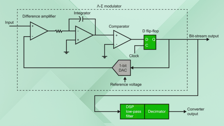
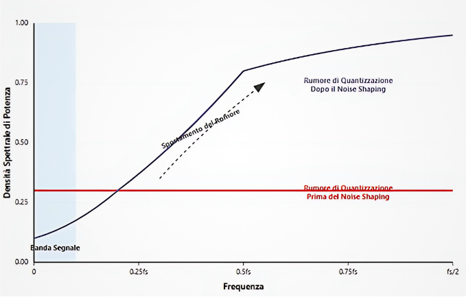
The Sigma-Delta architecture takes a radically different approach, based on oversampling and shaping of the quantization noise.
** **
**
Operating principle:
- The signal is sampled at a rate far higher than Nyquist
- A modulator made up of an integrator and a 1-bit quantizer generates a bit stream
- The quantization noise is shaped and pushed toward high frequencies
- A digital decimation filter removes the high-frequency noise and reduces the sample rate
This architecture makes it possible to achieve extremely high resolutions (up to 24 bits and beyond) at the expense of bandwidth.
Application case: a data-acquisition system for precision scientific measurements needs extreme resolution to detect tiny changes in low-frequency signals. A 24-bit Sigma-Delta ADC with an effective sampling rate of 10 SPS delivers resolutions down to 1 μV on a ±10V scale. The complete system integrates a front-end with a programmable-gain amplifier and ultra-stable voltage references. This configuration is ideal, for example, for resistivity measurements on superconductive materials, where infinitesimal changes can signal critical phase transitions.
Pipeline ADC
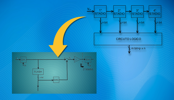 The Pipeline architecture is a compromise between Flash speed and SAR efficiency, implementing a sequence of partial-conversion stages.
Operating principle:
- The signal passes sequentially through multiple conversion stages
- Each stage resolves a few bits (typically 1 to 4)
- The residue is amplified and passed to the next stage
- The partial results are appropriately delayed and combined to form the final result
This architecture makes it possible to achieve high sampling rates while maintaining high resolutions (12-16 bits).
Application case: a video-acquisition system for medical imaging requires high resolution and high speed at the same time. A 14-bit Pipeline ADC running at 80 MSPS can digitize high-definition video signals while preserving details critical for diagnosis. In the practical implementation, the analog signal from the image sensor passes through a precision sample-and-hold circuit before entering the converter. Precise timing is ensured by a low-jitter clock system, essential for maintaining image integrity. This solution makes it possible to view high-resolution diagnostic images in real time, a fundamental capability in procedures such as angiography.
Key Parameters for Evaluating ADCs
Picking the right converter for a specific application requires understanding and evaluating many parameters that characterize its performance. Some are static in nature, others dynamic, and their relative importance depends on the application context.
Static Parameters
- Resolution: number of bits used to represent the digitized signal — determines the number of available discrete levels (2N).
- Absolute accuracy: maximum deviation between the actual analog value and the digitized one, accounting for all errors.
- Offset error: constant deviation between the ideal and actual value, independent of signal amplitude.
- Gain error: deviation proportional to the signal amplitude — a scale error.
- Differential nonlinearity (DNL): deviation of the actual width of a quantization step from the ideal width.
- Integral nonlinearity (INL): deviation of the transfer function from the ideal straight line.
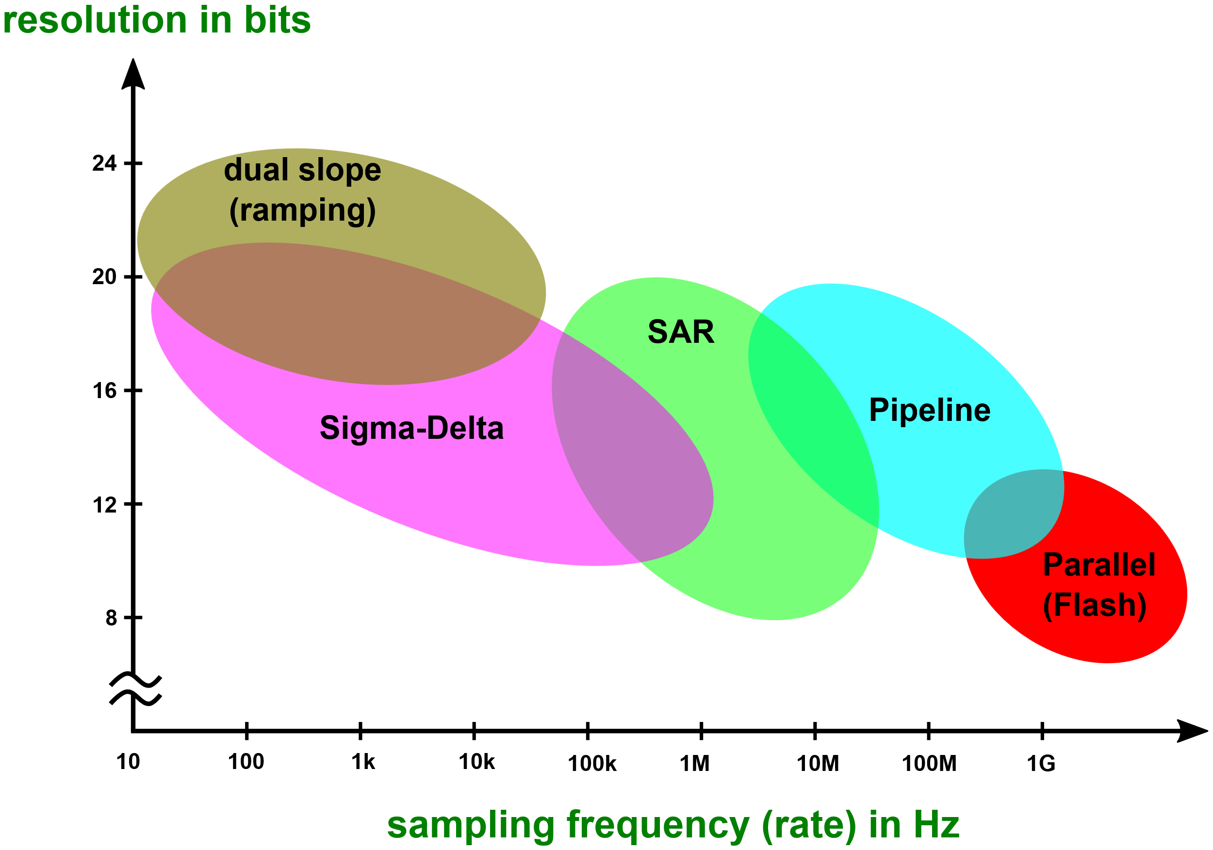
Dynamic Parameters
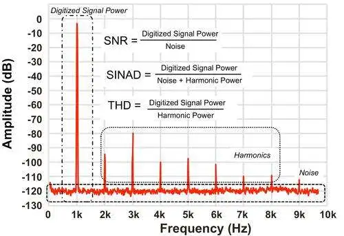
- Signal-to-noise ratio (SNR): ratio of signal power to noise power, expressed in dB.
- Total harmonic distortion (THD): measure of the harmonic components introduced by the conversion process.
- Signal-to-noise-and-distortion ratio (SINAD): combines SNR and THD into a single parameter.
- Effective number of bits (ENOB): estimate of the effective resolution considering the effects of noise and distortion.
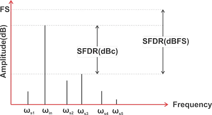
- Spurious-free dynamic range (SFDR): ratio between the amplitude of the fundamental signal and that of the largest spurious component.
- Aperture delay: delay between the sampling command and the actual sampling instant.
- Aperture jitter: random temporal variation in the exact moment of sampling.
**  **
**
Functional and Operational Parameters
- Sampling rate: number of samples acquired per unit time.
- Conversion time: interval required to complete a single conversion.
- Reference voltage: value that sets the converter’s full scale.
- Input impedance: load presented to the circuit providing the analog signal.
- Power consumption: energy required for operation, both in active and standby mode.
- Digital interface: communication protocol used to transfer the digital data (SPI, I²C, parallel, etc.).
Historical Evolution and Technology Trends
From the Origins to the Digital Era
Analog-to-digital conversion has roots that go back to the earliest telecommunication systems. However, only with the advent of integrated semiconductors did A/D converters start becoming widespread, accessible components.
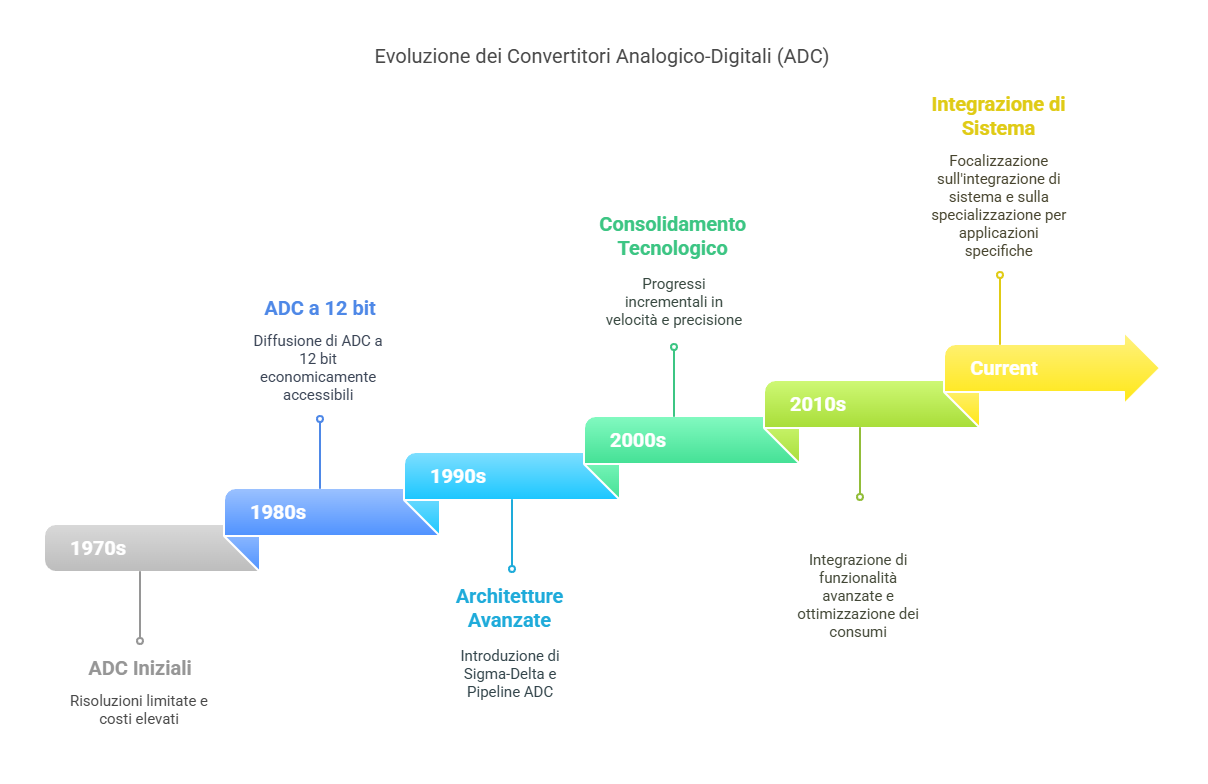
The first integrated ADCs of the 1970s offered limited resolutions (8-10 bits) with modest speeds and high prices. Technological evolution has led to progressive improvements across every performance metric, along a trajectory similar to Moore’s law for processors:
- 1980s: the first economically accessible 12-bit ADCs become widespread
- 1990s: introduction of advanced architectures such as Sigma-Delta and Pipeline
- 2000s: the technology consolidates, with incremental advances in speed and precision
- 2010s: integration of advanced features and power optimization
- Today: focus on system integration and specialization for specific applications
Current Technology Trends
- System Integration: modern ADCs rarely exist as standalone components; they are embedded in more complex systems that include analog multiplexers, programmable amplifiers, voltage references and advanced digital interfaces.
- Energy Optimization: with the proliferation of battery-powered devices, energy efficiency has become a critical parameter, driving the development of ultra-low-power architectures and advanced power-saving modes.
- Application Specialization: the industry is moving toward more specialized solutions, optimized for specific application domains such as biomedical, automotive, communications or instrumentation.
- Integration with Digital Processing: the rise of System-on-Chip architectures has led to tighter integration between conversion and digital processing, optimizing the entire data flow.
Conclusion: The Strategic Role of ADCs in the Digital Ecosystem
Analog-to-digital converters are one of the most critical elements in the interface between the physical and digital worlds. Their quality sets the upper limit on the performance a system can achieve, creating a fundamental “bottleneck” in the information flow.
A thorough understanding of operating principles, available architectures and performance parameters enables informed choices in selecting and implementing these critical components.
In the next articles of this series we’ll dive deeper into each of the main architectures, analyze characterization and testing techniques, explore practical implementation considerations, and discuss the most significant applications across various industrial sectors.
Key Takeaways
- Analog-to-digital conversion is a multi-stage process comprising sampling, quantization and encoding
- The Nyquist-Shannon theorem sets the fundamental constraints for faithful sampling
- Different architectures (SAR, Flash, Sigma-Delta, Pipeline) offer specific trade-offs between speed, precision and power
- A complete evaluation of an ADC requires considering both static and dynamic parameters
- Technology evolution continues to push toward greater integration, energy efficiency and application specialization
Suggested Further Reading
To dig deeper into the topics covered in this article, I suggest:
- Reading the next article in the series, focused on SAR and Flash architectures
- Exploring the technical specifications of commercial converters to see the practical interpretation of the parameters
- Getting familiar with simulation tools for modeling converter behavior
- Studying signal-conditioning techniques, essential to fully exploit the potential of ADCs